


Figure 1: Comparison of the normalized area of a chip versus the voltage rating of the best MOSFETs, in blue, with the latest generation of GaN FET (Source: Efficient Power Conversion (EPC))
From skepticism to game changer
Ten years ago, when GaN pioneers presented the concept of industrializing a disruptive technology aimed at offering a more efficient Gallium Nitride based alternative to super-junction MOSFETs, it attracted a lot of opinions and strong statements: “It will never fly”! As it has been for the digital power, the journey from ‘garage development’ to commercial products has been full of frustration, tears and deceptions, though the perseverance and strong believes in the technology have brought it to a successful state.
GaN high-electron mobility transistors (HEMT) have very interesting intrinsic behavior patterns, delivering superior switching performance and able to offer unprecedented levels of performance compared to conventional MOSFETs. In terms of intrinsic performance, having a very low charge gate, zero reverse recovery and flat output capacitance, GaN has everything that power designers dreamt of for decades to improve performance, decrease size and to reach the mythical 99.99 % efficiency.
One example of a benefit of GaN transistors is the die size, which is much smaller than conventional MOSFETs (Figure 1). The graph compares the normalized area of a chip versus the voltage rating of the best MOSFETs in blue, with the latest generation of GaN FETs. The separation in the die size ‘Figure Of Merit’ between silicon and GaN FETs is growing rapidly. It is now sits at 16 times at 200V and four times at 100V – and we may not have reached the limits yet. This opens the door for power designers to create higher integration and products that will literally amaze us with their performance levels. So much so in fact, it looks like we have truly entered a game-changing era!
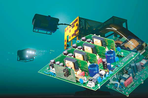
Figure 2: PRBX VB410-384 – Subsea power supply with full digital control power management, monitoring and intelligent redundancy. (Source: Powerbox)
Step by step to maturity
As it is for any new technology, especially when disruptive, moving from research to high volume production is a long process, one that includes new learning for electronic engineers and in the case of GaN, the implementation of zero-voltage switching topologies requiring very specific drivers and new ways to control them. Despite the huge benefits of GaN transistors, for many years the lack of drivers has limited the interest level from industrial designers. However, the increased number of semiconductors players investing in GaN in the last two years has made this technology simpler to implement.
Many technical barriers have been removed. Manufacturing processes have gradually been optimized to increase yield and reduce cost, quality processes specific to this technology have been implemented, and in November 2017 the JEDEC organization announced the formation of a new committee to set standards for Wide Bandgap Power Semiconductors (JC-70), which is a sign of readiness for mass implementation.
Step by step, the puzzle is going to be completed and if GaN has been widely used in LED and RF applications, it is now starting its journey in the DC/DC converters and AC/DC power supplies segments. There is not a week without a new product announcement and for sure a lot of things will happen during the next coming months.
Have you ever imagined?
Starting my career as a power supply designer in 1982, I have been through many technology shifts and I still remember the debates about the risks of moving from linear power supplies to switching ones. I was lucky enough to work for a large telecommunications company that began research into digital power when many considered it to be anecdotal, and I was happy to be amongst the pioneers exploring new ways to manage power conversion and to improve efficiency. Today, the combination of digital control and the unprecedented benefits of GaN are realizing a dream for all ICT board power designers, to manage the conversion from 48V to 12V in a footprint exceeding 1200W per cubic inch with an efficiency of 96 percent, and we haven’t seen the end of the GaN evolution.

Figure 3: PRBX GB350 – Coreless power supply operating in high magnetic field applications (MRI) fully digitally controlled and monitored (Source: Powerbox)
Celebrating 15 years of digital innovation
Today, digital power is part of most power engineers’ educational program and is implemented in a large variety of applications. It is important to remember the origins of digital power, and how from early research work conducted in the mid-seventies by Trey Burns, N.R. Miller and others, digital power gradually took its place in the power industry to reach a level of maturity that makes total sense for a designer to consider the technology. In the seventies, at a time when the power industry was slowly considering the migration from linear-power to switching-power, Trey Burns researched and explored the use of the State-Trajectory Control Law in Step-up DC/DC converters and he compared two methods of realization, one employing a digital processor and the other using analogue computational circuits. It is anecdotal but nonetheless interesting to note that at that time, an experimental product built by Trey Burns was a boost converter operating at a switching frequency of 100Hz – which sounds slow – but it had to be slow because it took up to 450 micro-seconds to execute the digital program per sample…
After more than 40 years from the days of initial research up to APEC 2018, and 15 years from the first commercial digital DC/DC converter presented in 2003, the technology, originally developed for the ICT industry, is now widely adopted by almost all segments of the industry. From monitoring and controlling deep sea power systems with the highest level of reliability (Figure 2) to guaranteeing stable voltages to critical medical equipment exposed to the high magnetic radiation of a Magneto Resonant Imagery system (Figure 3), digital power is almost everywhere, and soon to be embedded in an equipment installed on the International Space Station. For all the pioneers who have been engaged in this journey, this is an amazing situation and we are now seeing the same level of excitement with the development of Gallium Nitride devices.
5000W/inch3 and 99.99% efficiency
What makes power designers’ lives exciting is the ever-present level of innovation making it possible to improve performance levels, contributing to reducing our environmental impact and to build a sustainable society. We are flooded with news every day – the Internet of Things (IoT), autonomous and electrical vehicles, and many technical innovations – they will all require very efficient and compact power sources. 5000W per cubic inch and 99.99 percent efficiency might sound impossible to reach, but who in the mid-seventies would have imagined what we could, and have already achieved today when combining new topologies, digital control, new components such as GaN, and of course, the passion to innovate?

Author: Patrick Le Fèvre, Chief Marketing and Communications Officer
Powerbox | www.prbx.com
![]()