


This article is a technical introduction to the RZ/A family, the new embedded processor from Renesas. The device is available in a number of options and a number of configurations designed to give designers a broad choice when designing their TFT drive or GUI application. The article will go into some detail on the features of the RZ/A family, including a technical overview of the memory architecture that includes the world’s largest embedded RAM (up to 10MB) as well as a specially designed bus architecture to ensure fast bus throughput to the memory.
Author: Robert Kalman, Product Marketing Manager Industrial Communications Business Group, Renesas Electronics Europe GmbH
The device also features the 5th generation Video Display Controller from Renesas, which is not only capable of driving a screen up to WXGA size but also of supporting multiple additional functions in hardware which would often be executed in software, so as to allow for full operation at a lower clock speed. The device also features on OpenVG 1.1 compliant block and the article will go on to show how this can be used to improve performance and reduce memory overhead.
The RZ/A family from Renesas is an all new series of embedded MPUs aimed at the Human Machine Interface market. The RZ lineup from Renesas is a new direction taken in the embedded processing arena, based on the Cortex A9 core from ARM running at 400MHz and including all the right IP for creating a high end HMI application without involving the costs, effort and compromises involved in the current HMI application development.
Embedded MPU?
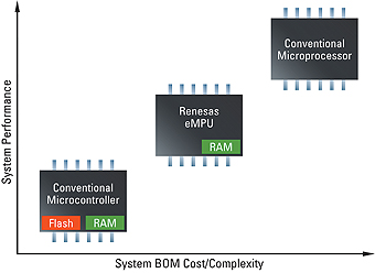
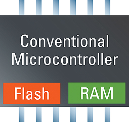
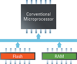
As well one may ask, what does the term “embedded MPU” actually mean? In order to answer this question, we have to have a brief look at the current offering across the MPU / MCU spectrum. Today, an MCU typically contains embedded flash and RAM, running code from the flash but somewhat limited in terms of performance, particularly when it comes to the area we are talking about – the performance level needed for a Human Machine Interface. The alternative today is the classical MPU or microprocessor system which achieves the performance level needed and can significantly exceed it; however, it typically will not have any internal flash and only a small amount of internal RAM. Typical MPUs have their place in the market as do MCUs, of this there is no debate. However, there is certainly a significant gap between the two areas.
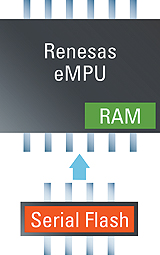
Filling the gap is where the eMPU can be useful. The eMPU, like an MPU, does not contain any embedded Flash and has a CPU core running at a performance that would not be possible with a typical MCU. This performance level can (as with the MPU) only be achieved by running from RAM. In contrast to the microprocessor system, which will use external RAM, the eMPU contains all the RAM that it will need for the application.
As can be seen in the system diagrams below, the MCU is obviously the most simple, but the eMPU offers a compromise offering the performance of an MPU without the complexity associated with it.
The eMPU typically will boot from an external serial flash, compared to an MPU, which will typically use external NOR flash. This can have several advantages:
• It is possible to use the QSPI serial flash block which can achieve even faster performance than the standard NOR flash.
• It requires less PCB space and fewer pins on the eMPU than a 32-bit parallel NOR flash.
The eMPU has enough RAM internally that it does not need to use external RAM, compared to an MPU which will typically use external DDR or SDRAM. This can have several advantages:
• The application is decoupled from the RAM market. Although this is not likely to be seen as a positive point for the average hardware designer, any purchasing team will breathe a sigh of relief to be free of this.
• It requires less PCB space and also fewer pins on the eMPU, and coupled with the use of a serial flash can allow designers to use a much smaller QFP package, allowing for a 2 layer PCB instead of a multi-layer PCB.
• It eliminates the requirement for an additional power supply of 1.8V for the DDR supply.
Now clearly there is a line whereby the performance of an eMPU is not going to reach that of the quad core multi-gigahertz system residing in a desktop PC, but not every HMI system today needs to be built like a PC. There is another way!
The features of the RZ/A devices
The RZ/A features a Cortex A9 core which is clocked at 400MHz and includes the optional IEEE754 compliant double precision floating point unit architecture (VFP) and the optional general purpose 128bit single instruction multiple data (SIMD) NEON extension. These extensions accelerate typical operations in DSP, multimedia and visualisation applications. The core, as is standard on Cortex A9 cores, has 32kB of instruction cache and 32kB of data cache. Additionally it includes 128kB of L2 cache to ensure that even if code is running from external non-volatile memory it can be executed at maximum performance.
The core alone is nothing unusual. The unique feature of this device is the inclusion of 10MB of internal RAM. This RAM is split into 4 separate blocks. Each block is 2MB in size and has a dedicated 128-bit wide bus running at 133MHz. This means that each block can be addressed concurrently by the different peripherals on the chip. At the same time as the CPU can be running code from one block, it can be writing data to a second block, whilst the third block can contain the picture data to be written to the TFT screen and the final block can be used for some DMA access or as the communications buffer for a TCP/IP stack; all of these with no bus collisions.
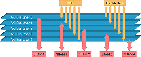
This is of course another major benefit of the eMPU architecture. Whilst an MPU has typically a fast bus to the external RAM, there is also only one of them. Thus the likelihood of a bus collision is high.
A feature of the 10MB of SRAM in the RZ/A family is the low-power RAM. In block zero of the RAM there is 128kB of “data-retention” RAM, which is also split down further into smaller blocks. These blocks can remain powered in low power modes and allow for a significantly faster wake up from these modes. The startup code and even the first screen to be driven to the TFT can be saved, thus as soon as the user presses a button or starts the system, it is as near as possible to a live state immediately. This is clearly another major advantage over MPU systems today which in order to achieve the lowest possible power consumption will remove power to the RAM and thus need to boot completely again from scratch.
Another unique feature of the RZ/A family is the SPI Multi-I/O. This peripheral can be thought of as a simple serial SPI block with a few extra enhancements. The first such improvement to the block is that it not only supports standard serial mode but also the new QSPI mode. This mode uses four parallel data lines as opposed to the standard 3 wire serial bus. With the new improved speed of this connection, initial benchmarks are showing a performance improvement in excess of 9 times when compared to the previous SPI modules. It also shows that it is possible to achieve even better performance (approximately 3%) than when accessing parallel external NOR flash, for example. This has the upshot of allowing for a fast boot time without needing to connect a 32-bit bus to a device. The other feature of the SPI Multi-I/O block is the “execute in place” functionality. The block allows the CPU to access the QSPI serial flash as if it were an external linear address space. This feature is also supported by the L2 cache, such that code can be run directly from this external flash. The upshot of this feature is that any critical code that needs to be run fast and regularly can be run from the internal RAM, and then code that does not need to be run regularly can be run from external flash. So although designers are limited to only 10MB of RAM, the amount of code that can be written is limited only to the size of the available external SPI flash.
Finally, from a communications point of view, the device comes with everything that you would expect. There is an Ethernet MAC, two USB 2.0 interfaces supporting both host and device functionality, as well as up to 5 CAN channels.
An overview of the Graphics IP (Video Display Controller and OpenVG)
So now we have learned that the RZ/A family is a fast processor which achieves high performance based on the 10MB of internal memory, and a wide bus avoiding collisions. It also supports a number of peripherals supporting all the standard interfaces one would expect while also allowing system designers to design a system with a low bill of materials cost without compromising performance. All of this is nice, but it doesn’t get to the real crux of the target application yet. How do you drive the screen?
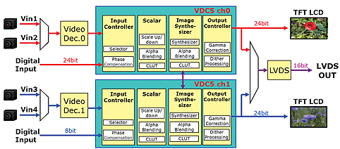
The RZ/A has two features which make driving a screen very simple and allow for an impressive GUI. The first of these features is the VDC5. The VDC5 is the 5th generation of the video display controller from Renesas and is able to drive screens up to a maximum size of 1999 pixels × 2035 lines, making it the most impressive of its kind. The VDC5 actually supports up to 2 channels meaning that two screens can be driven concurrently. The VDC5 also supports standard digital interfaces as well as LVDS, such that the trend in larger screens to use the LVDS interface can also be supported.
The first portion of the VDC is the input controller, which can receive up to two video input signals up to a maximum size of 1440 × 1024. The input controller supports phase compensation as well as horizontal noise correction and contrast correction. The input signals are then passed to the scaler block.
The scaler block (of which there are two per VDC5 channel) can be used to scale the two video inputs either up or down to create the correct size image for the screen. The images can also be rotated and the two video inputs can even be overlaid using alpha blending and a colour look-up table (CLUT). The final images (if both inputs are treated separately) or image (if only one input is used or the two inputs are overlaid) are then stored in a frame buffer in the RAM and passed to the image synthesiser.
The image synthesiser combines up to 4 individual layers to create a single image. When the either only one or no video inputs are being used, these layers are free to be used for other parts of the GUI as separate overlay layer or icons. Through a process of alpha blending and the CLUT, the final single image is created for the screen, and driven to the output controller.
Finally, the output controller takes the generated image and drives it to the TFT screen, either via the LVDS or the digital output, in one of many supported formats: RGB888 (24-bit parallel output), RGB666 (18-bit parallel output), RGB565 (16-bit parallel output) or RGB888 (8-bit serial output).
The operation of the alpha blending and the combination of the multiple layers means that the CPU can be offloaded of this functionality.
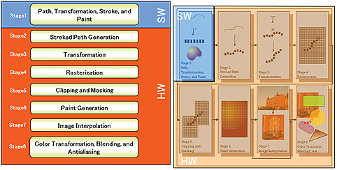
The second peripheral of the RZ/A devices that is useful for HMI development is the OpenVG-compliant graphics engine, which is a 2D vector graphics accelerator. The IP accelerates stages 2 to 8 of the OpenVG pipeline by using dedicated hardware and a compliance tested library.
The OpenVG engine can be used to fill the frame buffers and the VDC5 can then be used to drive the image data to the screen.
The advantage of using openVG is that it allows for the use of vector graphics, which can greatly improve the efficiency as well as the “look and feel” of a GUI.
Two simple examples can be used: where an image has to be rotated, the easiest way to do this with a bitmap image is to save the image 360 times, each rotated by 1 degree, and then simply show each picture one after the other.
This is clearly a significant overhead in terms of memory usage and also in terms of bandwidth of the device, while a vector implementation of the same picture can simply be rotated and the support for this rotation is included in hardware in the RZ device. The second example is that of scaling, and in this case a picture paints a thousand words, so I will leave the picture below uncommented.

Putting it all together
The RZ/A, Renesas’ new eMPU, is designed to fill the gap between the traditional MPU and the traditional MCU market spaces. It features up to 10MB of embedded SRAM, and supports a fast wake up from lower power modes. The device only needs a simple and low cost serial flash from which it can boot directly. The 10MB of memory is enough to store both the front and the back buffer for a double buffered HMI application. The RZ’s 10MB of internal RAM is connected to a multi-layered bus and is separated into 2MB blocks, such that the RAM can be both read from and written to by multiple sources concurrently. This enables a high performance Human Machine interface application to run on a system that needs no external RAM and has a low number of pins, available in QFP packages such that designers are able to use a 2 layer PCB.
The RZ/A will never achieve the simplicity of an 8 bit MCU with 16k of ROM, nor will it ever achieve the performance of a quad-core 2GHz Processor, but Renesas believes that your next Human Machine Interface application needs just a little bit more performance than a standard MCU can offer, but without making that big jump to a microprocessor architecture.
www.renesas.com