


 Objective
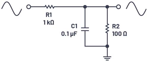
Figure 1. 11:1 attenuator/filter.
The objective of this activity is to investigate the simple differential amplifier using enhancement mode NMOS transistors.
The notes on hardware limitation issues presented in the June 2021 StudentZone article are valid also for this activity. The signal-to-noise ratio can be improved by increasing the signal level and then placing an attenuator and filter (see Figure 1) between the generator outputs and the circuit inputs. The materials needed for this activity are:
- Two 100 Ω resistors
- Two 1 kΩ resistors
- Two 1 μF capacitors (marked 104)
This attenuator and filter will be used in all parts of this lab.
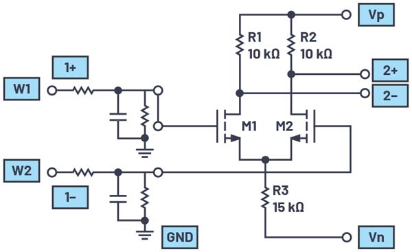
Figure 2. NMOS differential pair with tail resistor.
Materials
- ADALM2000 Active Learning Module
- Solderless breadboard
- Jumper wires
- Two 10 kΩ resistors
- One 15 kΩ resistor (use a 10 kΩ in series with a 7 kΩ)
- Two small signal NMOS transistors (CD4007 or ZVN2110A)
Directions
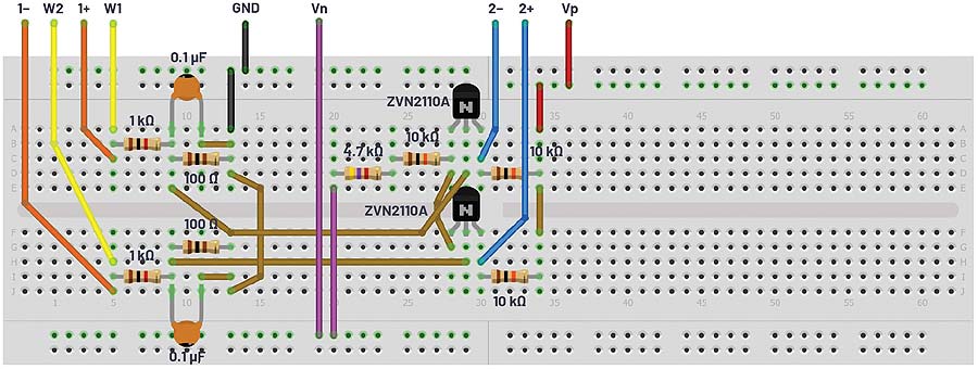
Figure 3. NMOS differential pair breadboard circuit.
The connections to the lab hardware are as indicated in Figure 2. M1 and M2 should be selected from the available devices with the best matching of Vth. The sources of M1 and M2 share a common connection with one end of R3. The other end of R3 is connected to the Vn (–5 V) and supplies the tail current. The base of M1 is connected to the output of the first arbitrary waveform generator, and the base of M2 is connected to the output of the second arbitrary waveform generator. The two collector load resistors R1 and R2 connect between the collectors respectively of M1 and M2 and the positive supply Vp (+5 V). The differential scope inputs 2+/2– are used to measure the differential output as seen across the two 10 kΩ load resistors.
Hardware Setup
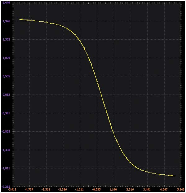
Figure 4. NMOS differential pair XY plot.
The first waveform generator should be configured for a 200 Hz triangle wave with 4 V amplitude peak-to-peak and 0 V offset. The second generator should also be configured for a 200 Hz triangle wave with 4 V amplitude peak-to-peak and 0 V offset but with 180° phase. Channel 1 of the oscilloscope should be connected with 1+ to the output of the first generator, W1, and 1– connected to W2. Channel 2 should be connected to display 2+ and 2– and set to 1 V per division.
Procedure
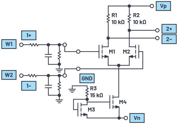
Figure 5. Differential pair with tail current source.
The following data should be taken: the x-axis is the output of the arbitrary waveform generator, and the y-axis is Scope Channel 2 using both the 2+ and 2– inputs. By changing the value of R3, the student can explore the effects of the level of the tail current on the gain of the circuit (as seen in the slope of the line as it passed through the origin) and the linear input range and the shape of the nonlinear curve fall off in the gain as the circuit saturates.
Using a Current Source as the Tail Current
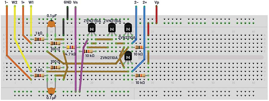
Figure 6. Differential pair with tail current source breadboard circuit.
Additional Materials
- Two small signal NMOS transistors (CD4007 or ZVN2110A for M3 and M4)
Hardware Setup
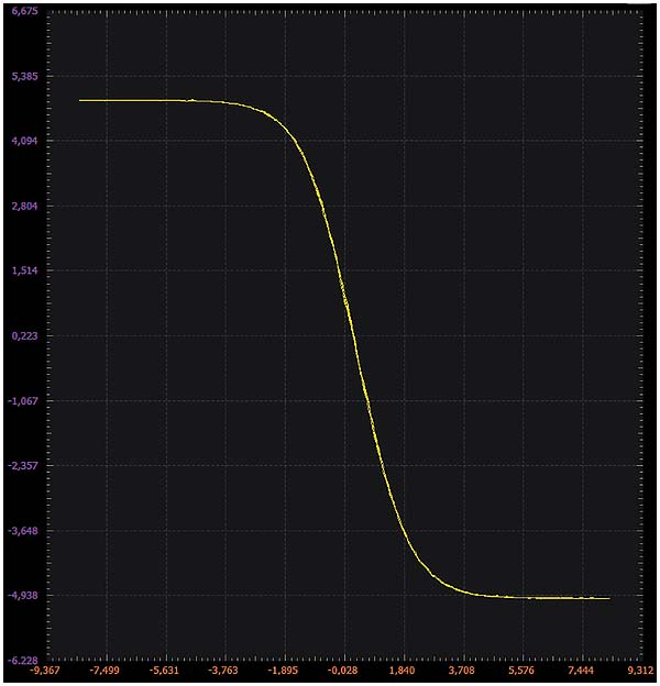
Figure 7. Differential pair with tail current source XY plot.
The first waveform generator should be configured for a 200 Hz triangle wave with 4 V amplitude peak-to-peak and 0 V offset. The second generator should also be configured for a 200 Hz triangle wave with 4 V amplitude peak-to-peak and 0 V offset but with 180° phase. The resistor dividers will reduce the signal amplitude seen at the bases of Q1 and Q2 to slightly less than 200 mV. Channel 1 of the oscilloscope should be connected with 1+ to the output of the first generator, W1, and 1– connected to W2. Channel 2 should be connected to display 2+ and 2– and set to 1 V per division.
Procedure
Configure the oscilloscope instrument to capture several periods of the two signals being measured. An XY plot example is presented in Figure 7.
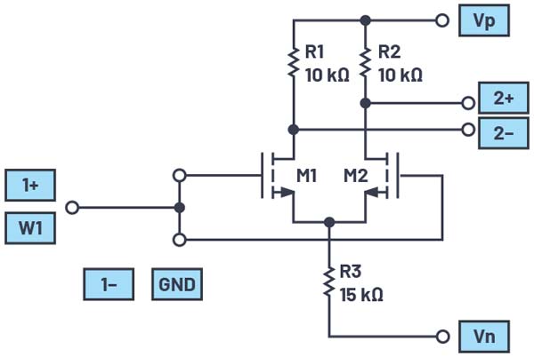
Figure 8. Measuring common-mode gain.
Measuring Common-Mode Gain
Common-mode rejection (CMR) is a key aspect of the differential amplifier. CMR can be measured by connecting the base of both transistors M1 and M2 to the same input source. Figure 10 shows the differential output for both the resistively biased and current source biased differential pair as the common-mode voltage from W1 is swept from +3 V to –3 V around ground. The gain will be affected the most as the transistors go from the saturation region to the triode (resistive) region as the positive voltage on the gates approaches the drain voltage. This can be monitored by observing the drain voltage single ended with respect to ground (that is, with the 2– input grounded). The amplitude of the generator should be adjusted until the signal seen at the output just starts to clip/fold over.
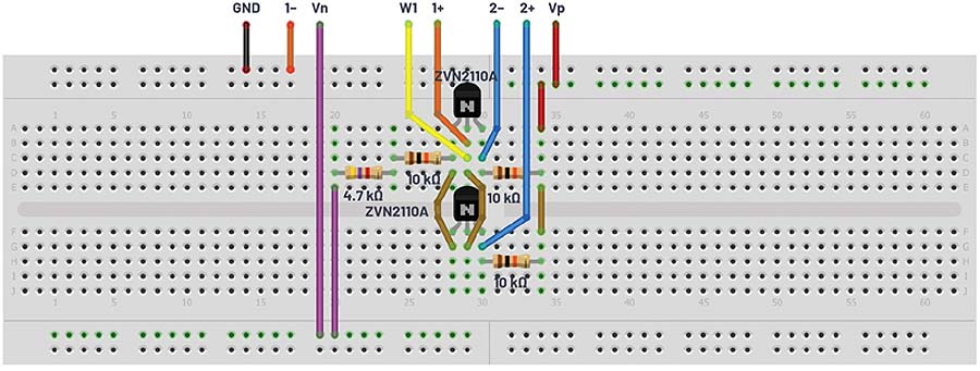
Figure 9. Common-mode gain breadboard circuit.
Hardware Setup
The waveform generator should be configured for a 100 Hz sine wave with 6 V amplitude peak-to-peak and 0 V offset. Channel 1 of the oscilloscope should be connected with 1+ to the output of the first generator, W1, and 1– to the ground. Channel 2 should be connected to display 2+ and 2– and set to 1 V per division.
Procedure
Configure the oscilloscope instrument to capture several periods of the two signals being measured. A plot example using LTspice® is presented in Figure 10.
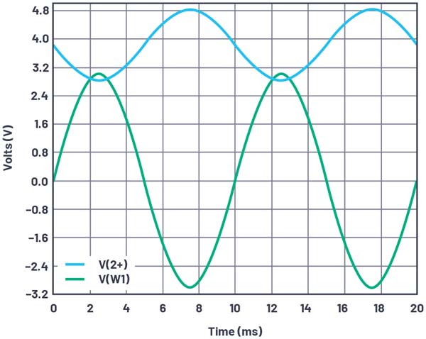
Figure 10. Common-mode gain waveform.
Questions:
- Would you characterize the transistor amplifier in Figure 8 as being inverting or noninverting to outputs 2+ and 2– with the base terminal of transistor M1 being considered the input? Explain your answer.
- Describe what happens to each of the output voltages (2+ and 2–) as the input voltage (W1) increases or decreases. You can find the answers at the StudentZone
About the Authors
 Doug Mercer received his B.S.E.E. degree from Rensselaer Polytechnic Institute (RPI) in 1977. Since joining Analog Devices in 1977, he has contributed directly or indirectly to more than 30 data converter products and he holds 13 patents. He was appointed to the position of ADI Fellow in 1995. In 2009, he transitioned from full-time work and has continued consulting at ADI as a Fellow Emeritus contributing to the Active Learning Program. In 2016 he was named Engineer in Residence within the ECSE department at RPI. He can be reached at doug.mercer@analog.com.
 Antoniu Miclaus is a system applications engineer at Analog Devices, where he works on ADI academic programs, as well as embedded software for Circuits from the Lab®, QA automation, and process management. He started working at Analog Devices in February 2017 in Cluj-Napoca, Romania. He is currently an M.Sc. student in the software engineering master’s program at Babes-Bolyai University and he has a B.Eng. in electronics and telecommunications from Technical University of Cluj-Napoca. He can be reached at antoniu.miclaus@analog.com.
![]()
Visit: https://ez.analog.com
Contact Romania:
Email: inforomania@arroweurope.com
Mobil: +40 731 016 104
Arrow Electronics | https://www.arrow.com
![]()