


Today’s market increasingly expects MCU with higher performance and lower power consumption. Low power implementation becomes the key challenge in SoC. Physical design is one of the critical phase to implement it. In this paper, we provide physical implementation methods base on Cadence Encounter Foundation Flow environment. The methods focus on SOG utilization increase or gate count decrease hence to reduce power dissipation. These methods include: floorplan adjustment, GigaOpt application, leakage power optimization, new version EDI application (13.12.000) and etc. These methods have general applicability. This paper also provides some examples with power reduction results for a mixed signal design on 90nm process.
Keywords: Low Power, Cadence EDI, GigaOpt, Leakage Power
Authors:
Savindar Fu, Freescale Semiconductor, Suzhou
Ken Du, Freescale Semiconductor, Suzhou
Alex Cai, Freescale Semiconductor, Suzhou
1. Freescale Kinetis Family Introduction
Freescale Kinetis is the first broad-market mixed-signal MCU family base on the ARM Cortex™ core and the most scalable portfolio of low power, mixed-signal ARM Cortex™ MCUs in the industry.
Kinetis MCUs are built on Freescale’s innovative 90nm Thin Film Storage (TFS) flash technology with unique FlexMemory. Kinetis MCU families combine the latest low power innovations and high performance, high precision mixed-signal capability. Kinetis portfolio consists of multiple hardware and software compatible MCU families with exceptional low-power performance, memory scalability including on-chip FlexMemory/EEPROM, and peripheral integration. Families range from entry-level to highly integrated and include a wide selection of analog, human-machine interface, connectivity, and safety and security functions. Kinetis MCUs are supported by a market-leading enablement bundle from Freescale and numerous ARM 3rd party ecosystem partners.
2. Kinetis Low Power Physical Implementation
2.1 Introduction
Kinetis MCU families combine the latest low power innovations and high performance with smaller chip size. On Feb. 25, 2014, Freescale announces the KL03 MCU, the world’s smallest and most energy efficient 32-bit MCU based on ARM® technology. The increasingly low power and small chip size requirement brings big challenge for backend physical implementation.
This paper provides physical implementation methods base on Cadence Encounter Foundation Flow environment. The methods focus on SOG utilization increase or gate count decrease hence to reduce power dissipation. These methods include: floorplan adjustment, GigaOpt application, leakage power optimization, new version EDI application (13.12.000).
2.2 Floorplan Adjustment
Hard block placement is one key factor which will impact final chip utilization. It’s time worth to adjust hard placement to get a good SOG shape for easier routing and higher density.
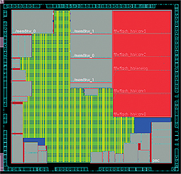
During back-end implementation of one Kinetis project, there is routing issue with below floorplan around red area (Flash hard block) and timing requirement cannot meet with this floorplan in figure 1. It will lead to die size increase if no smart adjustment.
• Each Flash have 64bit output for read data. There are 4 Flash in chip. From floorplan view, there is no enough space for routing. This cause congestion issue.
• Flash also have high frequency requirement according to high performance definition.
There are critical paths around Flash. Long distance routing cause worse timing.
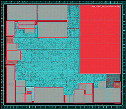
After deep analysis and much discussion, floorplan change to shape in figure 2.
• Keep enough space for Flash output routing.
• Keep enough space for Flash soft wrapper placement.
This floorplan shape makes routing and timing closure easier.
2.3 GigaOpt Application
Cadence® Encounter® Digital Implementation (EDI) system provides the most effective methodology to maximize performance, and minimize power and area for high-performance, 100M+ instance, and power-efficient designs. EDI System delivers the most comprehensive and deterministic solution for physical implementation and design closure of today’s most demanding chip designs.
GigaOpt is an ultra-fast and multi¬threaded/highly scalable optimization technology that provides better quality of results (QoR) with faster runtime. GigaOpt provides significant improvement in worst negative slack (WNS), total negative slack (TNS), and density while simultaneously reducing dynamic and leakage power across the board.
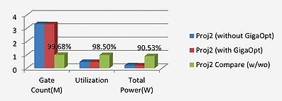
Below are different data that compares implementation with/without GigaOpt in two Kinetis projects. Tables compare the result for gate count, utilization, timing WNS/TNS and total power.
Project 1 is a small project showing in table 1. During analysis, it is split into two
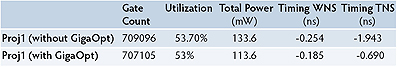
charts. One includes gate count, utilization and total power. Another includes timing information.
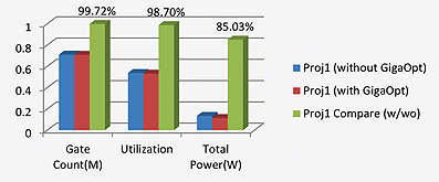
• Chart 1 compares three items.
– Gate count got 0.28% improvement with GigaOpt.
– Utilization got 1.3% improvement with GigaOpt.
– Total power got 14.97% improvement with GigaOpt.
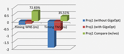
• Chart 2 compares two items.
– Timing WNS got 27.17% improvement with GigaOpt.
– Timing TNS got 74.49% improvement with GigaOpt.
Project 2 is a bigger projects showing in table 2. It also is split into two charts for analysis.
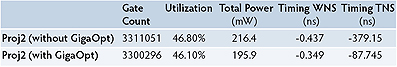
• Chart 3 compares three items.
– Gate count got 0.32% improvement with GigaOpt.
– Utilization got 1.5% improvement with GigaOpt.
– Total power got 9.47% improvement with GigaOpt.
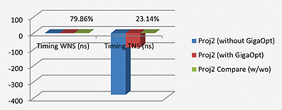
• Chart 4 compares two items.
– Timing WNS got 20.14% improvement with GigaOpt.
– Timing TNS got 76.86% improvement with GigaOpt.
From two projects analysis, GigaOpt will help backend to improve EDI performance.
2.4 Leakage Power Optimization
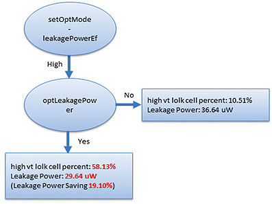
For 90nm and below technologies, leakage is the main factor which dominates over the dynamic power. Use optLeakagePower in EDI to optimize total leakage power of the design by swapping gates for gates with lower leakage power without degrading timing. Use this command after the design meets timing requirements.
This command resizes only those cells that have positive slack, unless a negative target slack is specified by the user.
Based on project 1, there is different result to show enable/disable leakage power optimization during EDI implementation in figure 3.
2.5 New Version EDI Application (13.12.000)
In EDI 13 release, GigaOpt technology is the default engine for optimization, including setup/hold/power optimization.
GigaOpt simplifies the timing closure flow.
For project 1, there is comparison between EDI 11.13 and EDI 13.12 for same design and database. The result is shown in table 3.
The result analysis also is split into two groups.
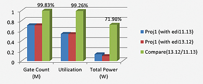
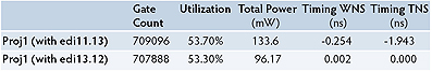
• Chart 5 compare three items:
– Gate count got 0.27% improvement with EDI 13.12.
– Utilization got 0.74% improvement with EDI 13.12.
– Total power got 28.02% improvement with EDI 13.12.
• Group 2 compares two items:
– Timing WNS got 0.256ns improvement with EDI 13.12.
– Timing TNS got 1.943ns improvement with EDI 13.12.
3. Issues and Workarounds
Cadence EDI System delivers the most comprehensive and deterministic solution for physical implementation and design closure. But EDI is not a impeccable tool. During Kinetis implementation there are issues which we have to find workarounds to meet the tape-out schedule.
3.1 Fix Hold Time
3.1.1 Issue Description
For timing optimization purpose, there are special delay cell which cell day is much bigger than buffer in our library. During hold time fix phase, EDI cannot smartly select delay cell firstly for big violations but inserts small buffer chain instead.
3.1.2 Workaround
During implementation, first step only use delay cells to fix big hold violations, then use buffers to fix remaining violations. This will reduce total gate count and area significantly.
3.2 Fix Transition Time
3.2.1 Issue Description
For some hard block pins with strict transition time requirement in timing model, EDI tool inserts buffer in each optimization stage, result in a redundant long buffer chain before those pins in the end.
3.2.2 Workaround
After placement, manually insert a big buffer for those pins and set don’t touch for them to prevent tool from optimizing. Check final database to find redundant long buffer chains and delete them to save gate count and area.
3.3 Critical Path Modules Placement
3.3.1 Issue Description
A part of Kinetis project have high frequency requirement. For some critical path related soft modules, EDI cannot smartly place them in a proper location thus lead to extra effort for optimization and gate count increasing.
3.3.2 Workaround
We need to provide some guidelines for tool during placement stage for better timing (createGuide, createDensityArea, createInstGroup and etc).
4. Conclusion
Freescale Kinetis projects face to embedded MCU market and there are many requirements for low power application. We use above methods in those projects with Cadence EDI new feature and new version to improve performance and also speed up run time.
Working with Cadence EDI, we will continue to improve the low power implementation flow to reduce power dissipation while keeping high performance ■
Reference
[1] Freescale, http://www.freescale.com
[2] Cadence, EDI System Text Command Reference
[3] Cadence, EDI System User Guide
www.freescale.com