


On-chip DAC operation
To allow designers to generate custom analog signals, microcontroller manufacturers have started including DAC peripherals on-chip. These can be used to generate precision voltages, as well as custom waveforms including sine waves and triangle waves. DACs can also be used for voice synthesis. A DAC generates an output voltage that is as low as 0 volts, and as high as the analog reference voltage for the DAC. The voltage is proportional to the digital value in the DAC data register, with a precision based on the resolution of the DAC. For example, if the DAC resolution is 8 bits, and the reference voltage is 5 volts, then the precision of 1 LSB of the DAC is 5/255 = 0.0196 volts. So ideally, if the 8-bit DAC data register contained 01h, then the DAC output would be the equivalent of 1 LSB, or 0.0196 volts. If the 8-bit DAC data register contains the value F1h (241), then the output of an ideal DAC would be 4.7236 volts. Ideally, adding 01h to the DAC data register should increase the value of the output voltage by 1 LSB.
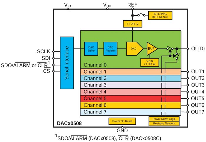
Figure 1 The DAC80508 interfaces to most microcontrollers using an SPI interface and has eight identical analog output channels. — (Image source: Texas Instruments)
Of course, just like any analog circuit, no DAC is ideal. The variation of the DAC output from the ideal value of the data register is called the differential nonlinearity (DNL) error and is measured in LSB. For example, a typical microcontroller DAC may specify a DNL of ±2 LSB.
DACs can also experience a linear gain error, measured as a percentage added to the ideal output, often adding an additional 0.5% to the output voltage.
For an ideal DAC, a plot of the output values against the DAC data register contents would be a straight line. Adding the linear errors caused by DAC circuit parameter variations for a real-world DAC would also be a straight line. In reality, that line would deviate from a straight line and would bow outward to form a non-linear curve. This non-linearity is also a result of variations in the DAC circuit over voltage and temperature. This non-linearity error is called the integral non-linearity (IRL) error. For microcontroller DACs this can be ±4 LSB or higher.
For frequency generation, the fastest output frequency of a microcontroller DAC is limited to the CPU frequency of the microcontroller.
All DACs require an accurate reference voltage to provide a precision analog signal.
On modern microcontrollers, that DAC reference voltage is usually derived from a dedicated analog reference voltage pin. Internal to the microcontroller, this analog reference voltage is kept separated and isolated from the internal digital logic to minimize power supply ripple. However, some small interference from the high-speed digital logic can be expected. While DAC peripherals are not as susceptible to power supply ripple when generating sine waves, this ripple can be noticeable when a stable and precise output voltage is required, or when generating a synthesized voice or musical tone.
While using a higher reference voltage can minimize the effect of power supply ripple, it would also prevent the DAC from generating smaller voltages, while also reducing the precision of the DAC for 1 LSB.
Single-chip external DACs for small signals
The DAC peripherals on most microcontrollers can provide sufficient accuracy for common applications. However, there are situations where extremely high precision and/or high speed is required. This is when an external DAC becomes a practical necessity.
Texas Instruments has a line of external DACs that can generate analog signals for any design problem. For example, if board space is scarce, the DAC80508MYZFT 16-bit DAC is extremely small at only 2.4 × 2.4 mm in a DSBGA package. This DAC has eight outputs and can interface to most microcontrollers using an SPI interface with a clock rate of up to 50 megahertz (MHz) (Figure 1).
The DAC80508 can use an external analog voltage reference or use the DAC’s digital power supply voltage to generate its own internal reference voltage of 2.5 volts with an accuracy of ±5 mV. Reference voltage drift is a minimal 2 parts per million per degree Celsius (ppm/°C). This provides a highly stable reference voltage over its -40°C to +125°C temperature range. Optionally, the reference voltage can be divided by 2 to provide analog signals with a 1.25 volt ceiling.
The DAC80508 has a precision not found on most microcontroller DAC peripherals. The INL and DNL are both ±0.5 LSB typical, ±1 LSB maximum. Gain error is ±0.5% typical, ±1% maximum. With 16-bit resolution, this level of accuracy is perfect for converting digital audio signals into analog audio. For example, it can be used to convert pulse code modulated (PCM) digital audio transmitted over fiberoptic cables or converting the digital audio from a storage device. After converting the digital audio into 16-bit audio data, the DAC80508 can convert the data to analog audio signals that are sent over common RCA cables. If the reference voltage is set to 1.25 volts, this is more than enough accuracy to generate line level audio signals.
The DAC80508 also has an output gain amplifier that can multiply the output voltage by two, generating an output voltage that is twice the reference voltage.
Generating analog waveforms with the DAC80508 through the SPI interface is simple. Every SPI command packet sent to a DAC data register is 32 bits wide. Each packet contains the channel address to be written to along with the 16-bit data to be written to the register. Any DAC80508 output channel can be programmed to either generate the output voltage immediately upon writing the data to the register, or it can hold all the values in the DAC data registers until the SPI writes to an internal broadcast register. Writing a logic “1” to any of the eight broadcast register bit positions updates only that DAC output with the value in its DAC data register. This allows for synchronous signals to be generated, useful for generating waveforms for test equipment.
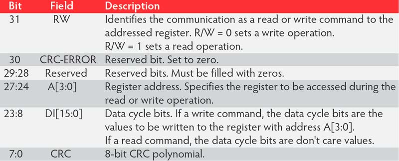
Table 1: Structure of the 32-bit SPI packet. When the DAC data register SPI packet of the DAC80508 contains an 8-bit checksum, the packet is sent MSB first, with the last bits (7:0) containing the checksum. The checksum is automatically generated by the DAC80508. — (Image source: Texas Instruments)
Avoiding signal errors and noise
When used in noisy industrial environments, occasional interference may be unavoidable, especially if high voltages are present. To prevent output signal errors as a result of interference on the SPI, the DAC80508 can optionally generate an 8-bit checksum at the end of every SPI packet (Table 1). If the checksum is valid, the DAC data register is written. But if the checksum fails, no data is written. Optionally, on a failed checksum, the DAC can pull the SPI SDO pin low, acting as an active low alarm pin. It is the responsibility of the microcontroller firmware to act on the failed checksum.
Regardless of the stated precision of any DAC, accuracy can only be assured by using a clean power supply. It is critical that VDD for the DAC80508 must be low noise with no ripple. If the DAC80508 is used in a DC-DC converter, extra care must be taken as these power supplies are by their very nature extremely noisy. Filtering on VDD is important, so a 1 microfarad (µF) to 10 µF capacitor, along with a 0.1 µF capacitor, must be placed between VDD and analog ground. Low ESR ceramic capacitors should be used and should be placed as close to the VDD pin as possible.
The analog signal outputs should be kept near the edges of the pc board and well isolated from the digital components. This serves not only to prevent interference on the DAC analog outputs, but also to prevent these analog signals from interfering with the other signals on the pc board.
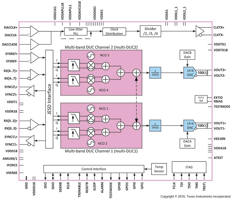
Figure 2: The DAC38RF82 is an ultra-high performance DAC that can generate waveforms in excess of 1 GHz. It interfaces to a host microprocessor using a low-power, eight lane JEDSD204B 12.5 Gbit/s interface. — (Image source: Texas Instruments)
High-speed, high performance DAC
Sometimes a no compromise application requires extremely high performance. DACs can even generate signals in the gigahertz range. This can be especially important for radar equipment when straight analog circuits cannot create the precision required for radar. For such applications, the Texas Instruments DAC38RF82IAAV high-speed RF dual-channel DAC can be used to generate waveforms above 1 gigahertz (GHz) in a relatively small 10 mm × 10 mm BGA package (Figure 2).
The DAC38RF82 supports three resolutions. When set for 16-bit resolution, it can generate RF signals of up to 2 GHz. When 12-bit resolution is selected, it can generate 2.66 GHz signals. The fastest mode is when it’s set to 8-bit resolution where it can generate 4.5 GHz waveforms. Certainly, these speeds are beyond the capabilities of any on-chip microcontroller DAC peripheral.
The DAC38RF82 has enough performance to be used in baseband transmitters such as cell towers, and can also be used for custom waveform generation for applications such as high-end test equipment. The DAC 38RF82 can also be used for radar signal generation for autonomous vehicles. This device is more complex than the DAC80508. Generating signals of up to 4.5 GHz requires a very fast data interface. The DAC38RF82 uses a JESD204B serial data interface that in 8-bit mode is as fast as 9 Gbits/s. At these interface speeds the device interfaces to an FPGA or an ASIC. When used in 12-bit or 16-bit mode, the DAC38RF82 can generate two RF waveforms. In high-speed 8-bit mode, only one waveform is supported. It requires three supply voltages, 1 volt, 1.8 volts, and -1.8 volts. Given the device’s typical application demands, these supply voltages must be very clean and ripple free. Ideally, each of the DAC’s three main and relatively independent sections – the digital subsystem, analog subsystem, and clock subsystem – would have its own partitioned power supply to avoid any unintended interactions.
The DAC’s DNL is ±3 LSB typical, its INL is ±4 LSB typical, and has a typical gain error of ±2%. Accuracy for a given application can be ensured by selecting the proper DAC data register values during testing.
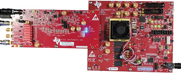
Figure 3: The DAC38RF82EVM on the left is fed digital data sent over a JESD204B interface generated by the TSW14J56EVM on the right, generating RF signals for testing. — (Image source: Texas Instruments)
Kickstarting DAC38RF82 development
When generating such high frequencies with sufficient accuracy, an evaluation board is an essential part of the development process. The DAC38RF82 is supported by the DAC38RF82EVM evaluation and development board, which supports all features of this high-end DAC. It requires a TSW14J56EVM data capture interface board to generate the digital signals that interface to the DAC38RF82EVM. The data capture board interfaces to a pc using a USB 3.0 interface.
The supplied evaluation software contains everything to evaluate, test, and program the DAC38RF82 for the target application.
When using such a high-speed device, layout is especially critical. The DAC38RF82 must be on the edge of the pc board and separated from all other components as much as possible. Short RF traces and the good practice bypass capacitors between supply pins and ground must be strictly followed. Other layout recommendations include the use of bypass capacitors with in-pad vias, with minimal stubs on those capacitors to avoid parasitic inductance. Also, designers should use a differential 100 Ω co-planar wave guide for output traces.
Conclusion
Microcontrollers with general purpose on-chip DACs are appropriate for generating reasonably accurate voltage and waveforms in the kilohertz range. However, for precision voltage or very high speed generation, external DACs can be used to significantly enhance application accuracy and performance, though some up-leveling of design practices with respect to power supplies and layout are also necessary.
 By: Rich Miron – Applications Engineer – Digi-Key Electronics
Rich has been in the Technical Content group since 2007 with primary responsibility for writing and editing articles, blogs and Product Training Modules. Prior to Digi-Key, he tested and qualified instrumentation and control systems for nuclear submarines. Rich holds a degree in electrical and electronics engineering from North Dakota State University in Fargo, ND.