


Introduction
One of the best ways to reduce electromagnetic interference (EMI) on PCB designs is through intelligent use of operational amplifiers (op amps). Unfortunately, op amps are often overlooked as a tool for reducing EMI in many applications. This may be due to the perception that op amps are susceptible to EMI and that extra steps must be taken to enhance their immunity to noise. While this is true of many older devices, designers may not be aware that newer op amps often have superior immunity performance over previous generations. Designers also may not understand or consider the key benefits that an op amp circuit can provide for reducing noise in their system and PCB designs. This article reviews sources of EMI and discusses op amp characteristics that aid in mitigating near-field EMI on sensitive PCB designs.
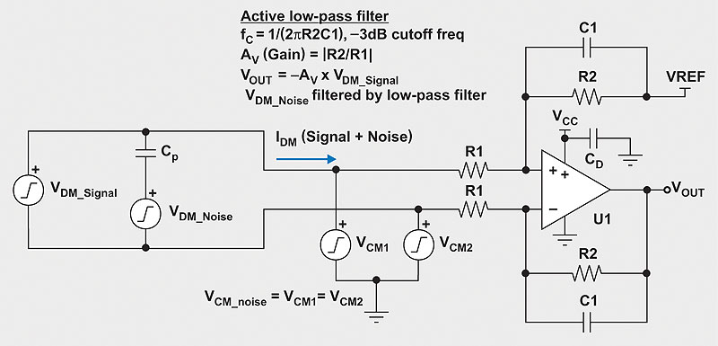
Figure 1: DM and CM input noise applied to active op amp filter.
EMI sources, victim circuits, and coupling mechanisms
EMI is a disturbance caused by a source of electrical noise that impacts a second electrical circuit in an unintentional and often undesirable manner. In all cases, an interfering noise signal is either a voltage, a current, electromagnetic radiation, or some combination of these three coupled from a noise source to a victim circuit.
EMI is not limited to radio frequency interference (RFI). Strong sources of EMI exist below radio bands in “lower” frequency ranges, sources such as switching regulators, LED circuits, and motor drivers operating in the tens to hundreds of kilohertz range. A 60-Hz line noise is another example. Sources transfer noise to victim circuits through one or more of four possible coupling mechanisms. Three of the four are considered near-field coupling, including conducted coupling, electric-field coupling, and magnetic-field coupling. The fourth mecha-nism is far-field radiated coupling, in which electromagnetic energy is radiated over multiple wavelengths.
Active filtering of differential-mode noise
Active op amp filters can significantly reduce EMI and noise on a PCB within the bandwidth of the circuit, but they are underutilized in many designs. The desired differential-mode (DM) signal can be band-limited while unwanted DM noise is filtered out. Figure 1 demonstrates DM noise coupled into an input signal through parasitic capacitance (CP). The combined signal and noise is received by a first-order active low-pass filter. The differential op amp circuit has its low-pass cutoff frequency set just above the desired signal bandwidth by R2 and C1. Higher frequencies are attenuated by 20 dB per decade. Higher-order active filters (for example, –40 or –60 dB/decade) can be implemented if more attenuation is needed.
Resistor tolerances of one percent or lower are recommended. Likewise, capacitors having very good tempera-ture coefficient (NPO, COG) and tolerances of 5% or lower are preferred for best filter performance.
Reducing input common-mode noise
In Figure 1, common-mode (CM) noise sources also present noise at the circuit’s input. CM noise can be described as a noise voltage that is common (or the same) at both op amp inputs, and is not part of the intended differential mode signal that the op amp is trying to measure or condition. CM noise can occur in a number of ways. One example is a system where the ground reference of one circuit is at a different voltage potential than a second circuit to which it is interfacing. The difference in “ground” voltages may be in millivolts or many volts, and can also occur at many different frequencies. These differences in voltages cause unintended voltage drops and flow of currents that can interfere with the connected circuitry. Cars, aircraft, and large buildings with many circuits are often susceptible to this type of interference.
A key advantage of op amps is their differential input stage architecture, and their ability to reject CM noise when configured as a differential amplifier. Common-mode rejection ratio (CMRR) is specified for every op amp, but total CMRR of the circuit must also include the effects of input and feedback resistors. Resistor variation strongly impacts CMRR. Therefore, matched resistors with tolerances 0.1%, 0.01% or better, are needed to achieve a desired CMRR for the application. While good performance is achievable using external resistors, use of instrumentation or differential amplifiers with internally-trimmed resistors is another option. For example, the INA188 is an instrumentation amp with internally trimmed resistors and high CMRR of 104 dB.
In Figure 1 the CM noise (VCM_noise = VCM1 = VCM2) can be rejected by CMRR of the op amp circuit if the noise is within the active bandwidth of the circuit. The level of rejection depends on accurately-matched resistors to be chosen for R2/R1. Equation 1 can be used to determine CMRRTOTAL, which includes the effects of resistor toler-ance (RTOL) and op amp CMRR as specified in the data sheet. For example, if the op amp data sheet specifies its CMRR(dB) = 90 dB, then (1/CMRRAMP) = 0.00003. In many circuits, resistor tolerance will be the main limiting factor to achieve a target CMRRTOTAL.
Equation 1 is derived from an equation in Reference 1 for CMRR of an ideal op amp, in which the CMRRAMP term is assumed to be very large (infinity).
 For an ideal op amp, the (1/CMRRAMP) term is zero and CMRRTOTAL is based only on resistors and AV. CMRRTOTAL can be converted to dB using Equation 2.
where AV = closed-loop gain of the op amp, RTOL = % tolerance of R1 and R2 (for example, 0.1%, 0.01%, 0.001%), and CMRRAMP = data-sheet specification for CMRR in decimal form (not dB).
Enhancing immunity to RFI and other high-frequency EMI
As shown in previous sections, active filtering and CMRR can reliably reduce circuit noise in the device’s band-limited range, including DM and CM EMI up into the MHz range. However, exposure to RFI noise above the intended operating frequency range may cause non-linear behavior in the device. Op amps are most susceptible to RFI on their high-impedance differential input stage because DM and CM RFI noise can be rectified by internal diodes (formed by p-n junctions on the silicon). This rectification creates a small DC voltage or offset that is amplified and may appear as an erroneous DC offset at the output. Depending on the accuracy and sensitivity of the system, this may create undesirable circuit performance or behavior. Fortunately, enhancing op amp immunity (or reducing susceptibility) to RFI can be achieved using one of two methods. The first and best option is to use an EMI-hardened op amp that includes internal input filtering to reject noise in the range of tens of megahertz up to gigahertz. More than 80 TI devices exist today and can be found by searching “EMI Hardened” devices on the TI op amp parametric search engine. More details on EMI-hardened op amps can be found in References 2 and 3.
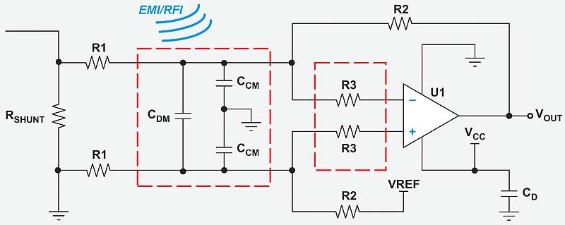
Figure 2: Passive EMI/RFI input filters improve high frequency immunity.
The second option is to add external EMI/RFI filters to the input of the op amp. This may be the only option if a design requires using a device that does not include internal EMI filters. Figure 2 shows a standard difference-amplifier configuration using external DM and CM filters that are targeted at higher EMI frequen-cies. Without input filters, the circuit gain is |R2/R1|. If passive input filters are added, R3 resistors are typically needed to prevent the CDM capacitor from reducing the phase margin of the amplifier. The DM low-pass filter consists of both R1 resistors, CDM, and both CCM capacitors. The CM low-pass filter uses both R1 resis-tors and both CCM capacitors. Equations for the –3-dB cutoff frequencies of the DM and CM filters (fC_DM and fC_CM) are shown below. fC_DM is set at a frequency above the desired bandwidth of the op amp circuit, and CDM is typically determined first. CCM capacitors are then chosen to be at least ten times smaller than CDM to minimize their impact on fC_DM, and because CCM capacitors are target-ing higher frequencies. As a result, fC_CM will be set to a frequency higher than fC_DM. Note that an EMI-hardened device can be used to eliminate the components boxed in red and simplify the design.
 Low output impedance reduces interference
Another important characteristic of op amps is their very-low output impedance, typically a few ohms or less in most configurations. To understand how this is beneficial for reducing EMI, consider how EMI impacts low- and high-impedance circuits. The diagram in Figure 3 represents two circuits. The first is an audio circuit that represents the input of an analog-to-digital converter (ADC) is comprised of a 1-VP-P, 2-kHz sinusoid (VS1), 600-Ω source impedance (RS1), and a 20-kΩ load impedance (RL1). Source impedances like 600Ω are common in audio applications for sources such as microphones and high-input impedances like 20kΩ are common for audio ADCs. The second circuit is a 100-kHz clock source driving a 3.3-V clock signal (VS2) with a series-termination resistor of 22Ω (RS2) and load imped-ance of 500kΩ (RL2). The high-impedance load repre-sents the digital input of another device. In a real system, I2C serial bus clocks in the 100- to 400-kHz range are common around audio ADCs and circuits. Although I2C clocks are typically driven in bursts (not continuously), this simulation shows the possible impact during the time the clock is driving.
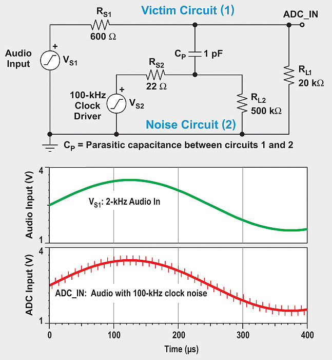
Figure 3: Clock noise source and audio victim circuit.
A clock routed near a sensitive audio trace is a real possibility on high density audio and infotainment PCB designs. For capaci-tive coupling to occur, it takes only a few picofarads of parasitic PCB capacitance to inject clock noise current into the victim audio signal. This is simulated using only 1pF of parasitic capacitance, as shown in Figure 3. How can noise be reduced in the audio circuit? As it turns out, reducing the impedance of a victim circuit is one way to reduce its susceptibility to coupled noise. For circuits with relatively high source impedance (>50Ω) coupled-noise can be reduced by minimizing the source impedance seen by the circuit load. In Figure 4, a non inverting configuration of the OPA350 is added to the circuit to buffer the signal and isolate the source impedance from the load. Compared to 600 Ω, the output impedance of the op amp is very low, which significantly reduces the clock noise.
Don’t forget the importance of decoupling
Adding decoupling capacitors to power supply pins is extremely beneficial in filtering high-frequency EMI noise and enhancing the immunity of the op amp circuit. All figures in this article show decoupling capacitor CD as part of the circuit. While the subject of decoupling can get complex very quickly, a few good “rules of thumb” apply to any design. In particular, select capacitors with the following characteristics:
(a) Very-good temperature coefficient, such as X7R, NPO, or COG
(b) Very-low equivalent series inductance (ESL)
(c) Lowest possible impedance over the desired fre-quency spectrum
(d) Capacitor values in the 1- to 100-nF range usually work well, but criteria (b) and (c) above are more critical than the capacitor value.
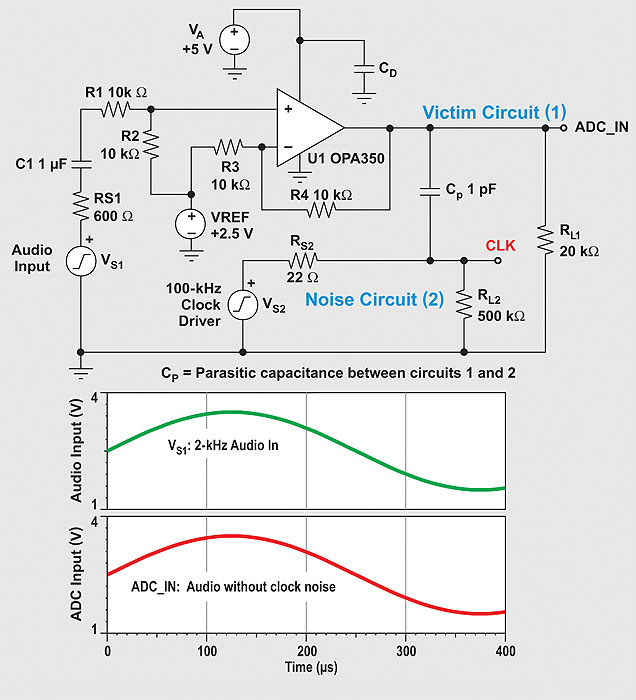
Figure 4: Op amp circuit reduces EMI from clock source.
Placement and connections are just as critical as the selected capacitor. Place capacitor as close to the supply pins as possible. Connections to PCB supply/ground should be as short as possible with short traces or via connections.
Conclusion
Op amps can help to reduce near-field EMI on a PCB and enhance the system design. Here are some key points to consider for any design:
• Reduce input DM noise from cables/circuits using a well chosen active filter configuration (Figure 1).
• Reduce input CM noise from cables/circuits by selecting an op amp with high CMRR and using precision matched resistors (Figure 1, Equations 1, 2).
• Further enhance immunity to high-frequency EMI or RFI (both DM/CM noise) by selecting an EMI-hardened device, or by using external passive EMI/RFI filters (Figure 2).
• Use the low impedance of the op amp output to reduce coupled noise when driving the signal to other circuits on the PCB.
• Finally, reduce supply noise by using a proper decou-pling strategy for the op amp and all other circuits.
References
1 S. Franco, “Circuits with Resistive Feedback,” Design with Operation Amplifiers and Analog Integrated Circuits, 3rd ed. New York: McGraw-Hill, 2002, Ch. 2, pp 75-76
2 Chris Hall and Thomas Kuehl, “EMI Rejection Ratio of Operational Amplifiers,” Texas Instruments Application Note (SBOA128), August 2011
3 “A Specification for EMI Hardened Operational Amplifiers,” Texas Instruments Application Note (SNOA497B), April 2013
4 Jerry Freeman, “Techniques to enhance op amp signal integrity in low-level sensor applications, Part 4,” EETimes, Dec. 18, 2008
Related Web sites
TINA-TI™ amplifier design tool: www.ti.com/tool/tina-ti
Product information: INA188 OPA350
Subscribe to the AAJ: www.ti.com/subscribe-aaj
Texas Instruments | www.ti.com