


 With the recent hype and the successfull releases of IoT products in the last years, many companies are put under big pressure to follow this hype and to take the initiative of coming up with own IoT products or to extend the existing product portfolio respectively. With the increasing number of nodes connected to the Internet, also the demand for low cost solutions with reduced BOM cost has increased. One way to overcome this, is the integration of the application MCU, network-processor and Wi-Fi radio in one IC. The so-called SoC (System on Chip) allows the implementation of a complete IoT application on a single device without the need of an external MCU. As no external MCU is required, this kind of operation is named hostless mode. The new QCA4010 from Qualcomm follows this approach and provides also special low power features and wake up scenarios .Wistron, as an ODM partner, has released a Wi-Fi module (DNSA-MP1) that is based on the QCA4010.
The QCA4010 integrates an Xtensa CPU @ 130 MHz from Tensilica that is responsible to provide all IP services and to manage all Wi-Fi links. The QCA4010 provides no internal Flash, but SRAM and ROM. Therefore the network processor code, system configuration and persistent data sets are loaded from external serial flash memory into the internal SRAM before execution. The application code is executed on the same CPU and memory ressources like the network processing code. Because the sesnor measurement, actor control and data processing handled by the application is normally done before a Wi-Fi link is established for data snychonisation, there is no bottlneck from the processing point of view. So in the most IoT applications, network and application processing is done in a time division manner by the CPU. But even if there is a demand to process both at the same time, the performance-rich 32 bit architecture of the Xtensa CPU together with the clock speed of 130 MHz provide sufficient calculation power to overcome this demand.
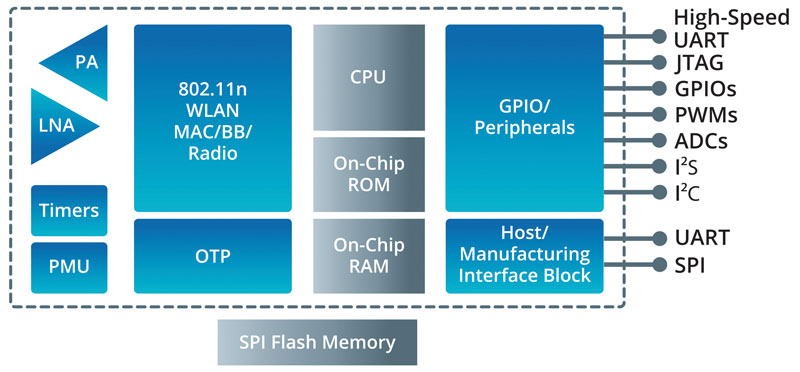
QCA4010 System Architecture
To fulfill the different application memory requirements in the IoT world, the QCA4010 is released in two SRAM versions. The smaler version integrates 1 MB SRAM, whereas ~400KB is reserved for application code. The bigger version provides 1.5MB, which allows the integration of ~800KB application code.
In order to reduce power consumption to a minimum, the QCA4010 provides an integrated Power Management Unit (PMU) that controls different power modes based on the following techniques:
• Gating Clock: Not required function blocks are disconnected from the clock network in order to prevent charge-reversal currents of parasite capacities.
• Shut down High Speed Clock: When the high speed clock network is not needed, it can be entirely disconnected, including external pulse sources such as oscillators.
• Reduction of the voltage level: The voltage levels of individual blocks can be reduced in order to keep the static leakage currents low. A minimum voltage guarantees a short wake-up time and maintains the data contents of all registers and of the volatile memory.
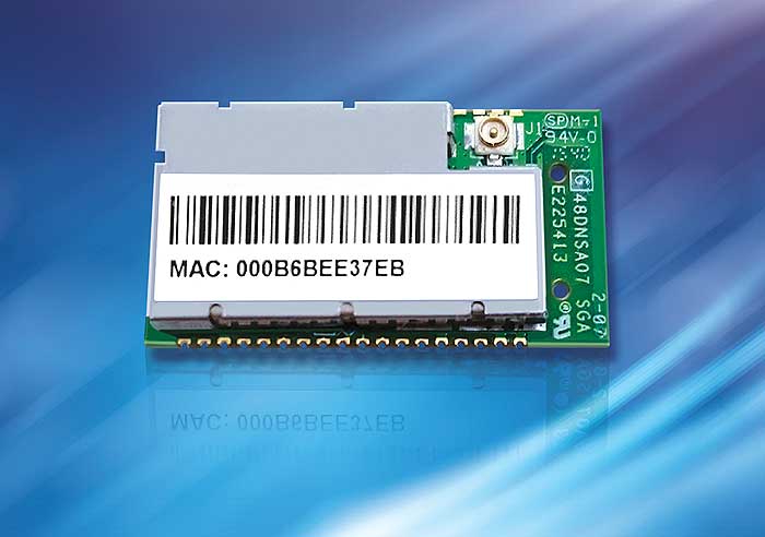
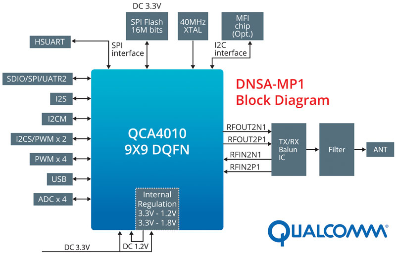
DNSA-MP1: Wi-Fi module based on QCA4010
The different low power modes are also supported by a low speed clock network (32.768 kHz) and a wakeup manager unit. The low speed clock network is required to run the state machine and sleep timers. The wakeup manager resumes operation by detecting internal and external trigger signals. For example, in supend mode it detects a wake up signal at a pin or from the internal sleep timer, after a predefined time has passed. In this mode it manages also a small RAM that stores state information. Further modes like POWER DOWN (~9µA), SLEEP and HOST_OFF extend the range of configurations and allows a fine power tuning of an IoT application. But even in network operation, when the CPU is running at high speed clock and a Wi-Fi link is operating, the user profits from the low power features like Green Tx power saving mode and low power listen mode supported by the radio.
The QCA4010 provides many different interfaces that are required in typical IoT applications. For the measurement of analog sensors, a 12 bit ADC with 8 channels supports 400ksps for multiple channels and 1 Msps for single channel operation. 8 independent 18 bit resolution PWMs with 8 bitclock prescaler are also available for e.g. motor control and lighting. For serial communication the user can chose from HS UART (3 Mbps), low speed UART, SPI, I2S or I2C as well. The following list gives an overview about the features:
• Support for IEEE 802.11b/g/n
• Single stream 1 × 1
• Single-band 2.4 GHz
• Integrated PA, LNA, with support for external PA and external LNA
• Single or dual Rx front end for antenna diversity
• Green Tx power saving mode
• Low power listen mode
• Data rates up to 150 Mbps
• Full security support: WPS, WPA, WPA2, WAPI, WEP, TKIP
• 8 channels 12-bit accuracy ADC, maximum sampling rate is 400 Ksps for multiple channels and 1 Msps for single channel.
• 8 18-bit resolution PWM with 8-bit clock prescaler
• 9×9mm DRQFN-116pin
• Case temperature range: 0°C to 85°C (standard); -45°C to 115°C (extended)
 For dual band application (2.4GHz & 5GHz), Qualcomm offers the QCA4012, which has exact the same system architecture and features like the “small” brother QCA4010, but provides just an additional 5GHz radio path. Therefor both parts are available in the same 9mm × 9mm × 0.9mm Dual-Row Quad Flat pack Nolead (DRQFN) package that includes a ground pad for improved grounding, mechanical strength, and thermal continuity. Moreover both parts are even pin compatible. But it should be mentioned that the concurrent mode is not supported by the QCA4012 as only one WiFi link (2.4GHz or 5GHz) can be served at a time. Anyhow, both devices (QCA4010 & QCA4012) support Rx diversity in the case that two Rx antennas are connected to the devices.
Quaclomm is an IC but not a PCB module supplier. Therefore Qualcomm works very closely with ODM partners like Wistron, which manufacture and sells Wi-Fi modules based on the original reference designs/ modules from Qualcomm. In case of QCA 4010, Wistron offers a module with the part number DNSA-MP1. MP1 is Qualcomm’s internal name for the QCA4010 reference module. Wistron has extend this part number with the prefix DNSA- to create an internal one. Documentation, SW and technical support is provided by Qualcomm, whereas Wistron provides the HW and the test reports based on the module name DNSA-MP1.
DNSA-MP1 Specification
• QCA4010 based Wi-Fi module
• 2.4GHz IEEE 802.11b/g/n, single stream 1×1
• 11n support for HT20 and HT40 bandwidth
• Internal PA and LNA, with external RF Switch for antenna diversity
• Green Tx Power Saving Mode, Low Power Listen Mode
• Up to 800KB of on-chip memory available for customer application
• Integrated IPv4/IPv6 networking stack
• Full security support: WPS, WPA2, WEP, SSL, etc.
• Built in protocol stacks: HTTP, DHCP, DNS, NTP, etc.
• 30mm x 16mm size, 4-layer
• Printed antenna or U.FL connector
• Single power supply: 3.3V
• Operation temperature: -40°C to 85°C (Industry Class Version)
• Regulatory compliances: CE, FCC
Contact:
André Ehlert – Tel: +49 89 130143811
e-mail: andre.ehlert@codico.com
CODICO | www.codico.com | https://www.codico.com/shop/en/highlights.html
![]()