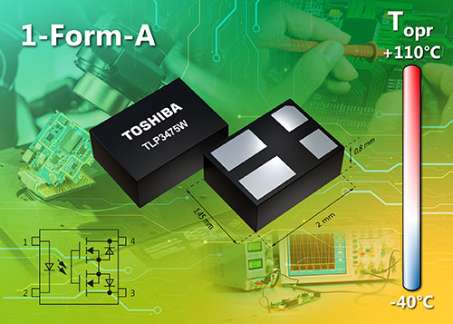
 Toshiba Electronics Europe GmbH (“Toshiba”) has launched a new photorelay specifically engineered to reduce insertion loss and suppress power attenuation of high frequency signals. The new device is intended for use in semiconductor testing applications including high-speed memory testers, high-speed logic testers or probe cards.
Through optimized package design, the new TLP3475W has reduced parasitic capacitance and inductance, thereby reducing insertion loss of signals in the frequency range 20GHz (typ.). This represents a 1.5x improvement in performance over the existing TLP3475S device.
The current (IFT) required to drive the LED is <3.0mA and on-state resistance (RON) is typically 1.1Ω. The isolation voltage (BVs) exceeds 300Vrms and output capacitance (COFF) is less than 20pF, contributing to switching times in the region of 2ms. It offers a normally open (NO) / 1-Form-A function.
The new TLP3475W is housed in a WSON4 package measuring just 1.45mm x 2.0mm x 0.8 mm (typ.), making it one of the smallest photorelays currently available. This is 40% smaller than Toshiba’s ultra-compact S-VSON4T package and is of particular value in multi-channel designs where multiple devices are deployed on a single card.
Operating temperature range is -40ºC to +110ºC, making it suitable for industrial applications, including high-speed semiconductor testing.
Learn more about TLP3475W here: https://toshiba.semicon-storage.com/eu/semiconductor/product/isolators-solid-state-relays/photorelay-mosfet-output/detail.TLP3475W.html
Volume shipments of the new photorelay start today.


