


 Anatomy of Phase-Locked Loop Circuits
Phase-locked loop (PLL) circuits are commonly found in many frequency generation devices. These devices ensure that the waveforms and signals created within the device are phase aligned or locked to a reference signal. Figure 1 shows a simplified block diagram of a PLL. The output of the voltage controlled oscillator (VCO) is divided using an N counter and compared to a reference signal using the phase/frequency detector (PFD) circuit. This simple circuit has been a subject of numerous textbooks and extensively studied. We will use some of the well-known basics to establish what it takes to drastically reduce the phase noise at the output.
Imperfections or phase noise of each building block contribute to the overall phase noise of the PLL circuit. The phase noise associated with each block can be modeled, and the overall phase noise of the PLL can be precisely predicted both through simulations and analytical calculations. Let’s review each of these blocks and discuss how they impact the output phase noise.
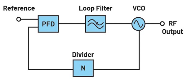
Figure 1: A phase-locked loop circuit.
The PFD block compares the reference signal to the divided output frequency. This block produces an error signal that is fed to a charge pump circuit that creates a control voltage, steering the VCO until the output phase of the device matches the reference phase. Most modern frequency generation devices with integrated PFD circuits provide a figure of merit (FOM) in their data sheets. Using the FOM, the in-band phase noise can be calculated as follows:
![]()
Where fPFD is the PFD frequency, and N is the value of the output frequency divider. Notice that the output frequency is a multiplication of the fPFD and N divider value. For a given output frequency, as the fPFD increases by a factor, the N value decreases by the same factor. This would result in a lower overall output phase noise since any reduction in the N value would reduce the phase noise by twice the rate of the increase due to the fPFD term. We can conclude that the higher the PFD frequency is, the lower the close-in phase noise will be. We will exploit this finding in the following sections of this article.
The loop filter follows the PFD and smooths the error signal originating from the PFD device that steers the VCO. It is designed by using several parameters of the system, such as the charge pump current, VCO sensitivity, and the PFD frequency. One of the less emphasized functions of the loop filter is that it determines the bandwidth of the negative feedback control loop. The reference signal will have an influence at the output signal’s phase noise within the control bandwidth of the loop filter. Beyond this cutoff frequency, the overall phase noise performance will be defined by the VCO characteristics. We will utilize this fact in the following sections to optimize the overall phase noise of the system.
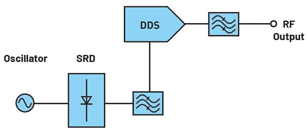
Figure 2: Variable frequency generation using a fixed source.
The VCO creates the output frequency based on the control voltage applied at its input. The VCO output frequency is updated by the control loop until it is phase-locked to the reference signal’s phase. The VCO directly influences the overall phase noise of the system. In general, as the quality factor of the VCO increases, its phase noise becomes lower. However, a higher quality factor usually requires components that usually limit the overall tunability range. VCOs that are tuned for a narrow frequency operation typically have the best phase noise performance.
Frequency Generation Options
There are many ways to generate signals using various oscillator topologies with varying levels of quality. Instrumentation applications typically strive for the best performance both in terms of low phase noise and spurious levels. Let’s review some frequency generation options that can achieve very low phase noise.
Frequency Generation Using Fixed Frequency Oscillators
One class of signal generation devices that have an excellent phase noise performance is fixed frequency oscillators. These devices typically have very high quality factors, enabling superior close-in phase noise performance. These oscillators operate at a predetermined frequency largely defined by the geometry and the construction of the device with some tunability to enable phase locking to a reference source. Oven controlled crystal oscillators (OCXOs), temperature compensated crystal oscillators (TCXOs), and voltage controlled SAW oscillators (VCSOs) are some examples of these types of devices. One key disadvantage of fixed frequency oscillators is the limited frequency coverage of these devices. While they may be suitable for devices that operate at a fixed set of frequencies or their multiples, most instrumentation devices require variable frequency coverage.
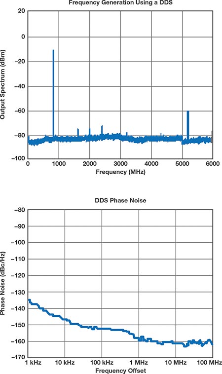
Figure 3: Output spectrum and phase noise of the AD9164 at 800 MHz using a fixed frequency oscillator as the sampling clock.
One solution to this problem involves using a direct digital synthesis (DDS) or a digital-to-analog converter (DAC) device. The fixed frequency signal can be used to drive the sampling clock of a DDS device, as shown in Figure 2. The oscillator’s frequency can be multiplied as needed through a frequency multiplier or a step recovery diode (SRD) and filtered before it is applied to the DDS. The DDS can create any arbitrary frequency up to half of the sampling frequency in the first Nyquist zone of operation. Some modern DAC devices can even operate comfortably in the second Nyquist zone. Figure 3 shows an example output spectrum and phase noise plot of the AD9164 driven by a low phase noise dielectric resonant oscillator (DRO) at 6 GHz. The phase noise plot shows an incredibly low output phase noise, and the output spectrum has spur levels less than –70 dBc.
Spectral purity of the multiplied sampling clock has a direct influence at the output of the device. Once the signal is multiplied, many harmonics will be present at the output. The desired signal needs to be filtered to achieve very low spurious levels at the output of the DDS. Typically, the spurs present at the sampling clock will appear at the output at similar levels. For large multiplication factors, the filters may need to be extremely sharp, which can require a significant area.
Additionally, the phase noise of the multiplied signal increases as the multiplication factor increases. For example, every time the signal’s frequency is doubled, the phase noise increases by 6 dB. Based on the starting phase noise profile and multiplication factor, the noise floor (far-out phase noise) could increase significantly, making the overall solution less appealing. This is a well-known dilemma where leveraging close-in phase noise of a single frequency, high quality factor device comes with a far-out phase noise floor penalty. As an example, surface acoustic wave (SAW) devices have excellent close-in phase noise performances with carrier frequencies around 1 GHz. A millimeter wave device operating above 40 GHz would require multiplication factors as high as 40. This could result in a 32 dB or more increase in the phase noise floor, which could make the solution less appealing.
Frequency Generation Using Wideband PLL Devices
Wideband synthesizers solve many of the challenges associated with single frequency devices. These devices, such as the ADF4372 microwave synthesizer, use multiple VCO cores that are further divided into multiple overlapping bands. This architecture enables each core and band to achieve a high quality factor. This significantly improves the overall performance of the device compared to the architectures utilizing a single core.
One key advantage of these devices is the higher fundamental operating frequencies compared to crystal or SAW-based oscillators. Many modern VCOs can have fundamental frequencies ranging from 4 GHz to 20 GHz and higher. This makes their far-out phase noise in millimeter wave applications much more appealing. For example, a device operating at 10 GHz fundamental frequency requires a factor of 4 to extend the frequency to 40 GHz. This translates as a phase noise floor increase of 12 dB, as opposed to the 32 dB increase with a crystal oscillator.
One challenge associated with these multicore and multiband devices is finding the optimum band to synthesize the target frequency. This could involve creating lookup tables to identify the correct band. Devices equipped with autocalibration features, such as the ADF4372 and ADF5610, make this process much easier and robust with temperature and process variations. This vastly simplifies the overall operation of the device where frequency changes can be simply programmed into the registers of the device and the most optimum band of operation is automatically determined.
Another challenge with this option is that the close-in phase noise associated with these devices is typically much higher compared to the single frequency devices. Even with the lower overall phase noise floor, the higher close-in phase noise can translate as higher overall integrated noise. This can limit the use of these devices in applications that demand lower integrated phase noise.
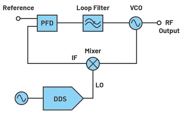
Figure 4: Translation loop architecture.
Translation Loop
The translation loop method takes the best of all the frequency generation methods reviewed earlier without taking their disadvantages. Let’s summarize what we have discovered so far before discussing the details of the translation loop.
Single frequency devices such as OCXOs, SAWs, and crystals with high quality factors have the best close-in phase noise. These single frequency devices usually have low fundamental frequencies, making their far-out phase noise less appealing when they are multiplied to millimeter wave frequencies. An ideal solution can take the close-in performance of these devices without the far-out phase noise penalty.
DDS or DAC devices can be used to generate variable frequencies using fixed frequency devices. These devices also suffer from large multiplication factors needed for millimeter wave frequencies and filtering needed to reject subharmonics and other undesired spurs. Tolerating these shortcomings can enable a desirable solution.
Wideband synthesizers can have very high fundamental frequencies with excellent far-out phase noise performance. However, these devices don’t really have high quality factors, making their close-in phase noise relatively poor compared to single frequency devices. Leveraging their far-out phase noise without the degraded close-in phase noise would be necessary.
This brings us to the translation loop device, as shown in Figure 4. Instead of dividing the output frequency by a large divider value, a frequency mixer is used to shift the output signal to an intermediate frequency (IF) that matches the reference signal’s frequency. This effectively reduces the divider value to 1, eliminating the noise contribution originating from typically large divider values used in traditional PLL devices. This also imposes the phase noise profile of the LO on the control loop. We can use a single frequency device with excellent close-in performance and a DDS to create this LO signal.
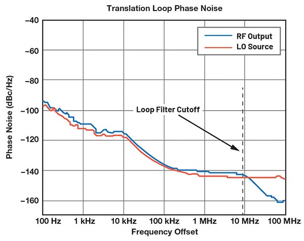
Figure 5: Phase noise profile of a translation loop device.
The loop filter bandwidth is a critical design parameter for the translation loop device. As we discussed earlier, the loop filter determines the overall bandwidth of the control loop. In other words, it defines how far the reference and LO signal have an influence over the output phase noise. We can choose a large loop filter bandwidth in the translation loop case since the close-in phase noise can be extremely low. Figure 5 shows the phase noise profile of a translation loop device and its LO input. Notice that while the LO has an extremely low close-in phase noise, the far-out noise floor is high. The RF output tracks the LO phase noise up to the loop filter bandwidth. After this frequency offset, the far-out phase noise is defined by the VCO, which is extremely low.
The translation loop device essentially leverages the desirable close-in performance of a single frequency device using a DDS device as an LO and utilizes the far-out phase noise of a wideband VCO by selecting a large loop bandwidth. This not only breaks the well-known dilemma about which phase noise region to optimize, but also results in an extremely low output phase noise.
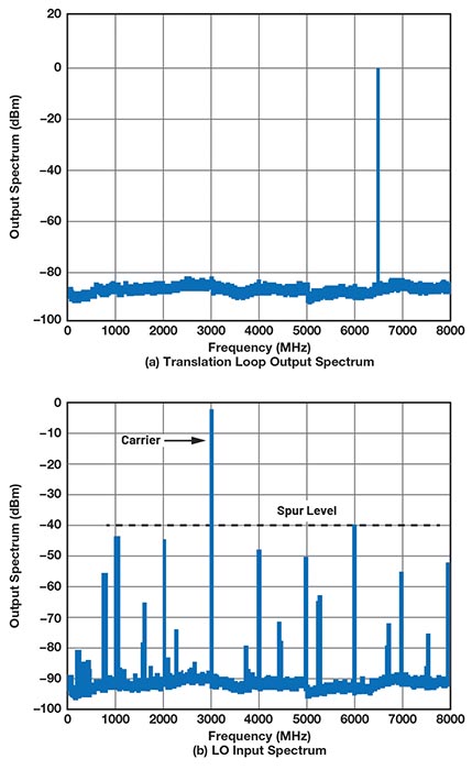
Figure 6: (a) Translation loop output spectrum at 6.5 GHz, and (b) LO input spectrum at 3 GHz. Using the internal LO frequency doubler of the ADF4401A, the effective LO frequency becomes 6 GHz. In this example, the IF frequency is at 500 MHz.
The superior phase noise performance of the translation loop makes it very useful in many millimeter wave instrumentation applications. In addition to the phase noise performance, instrumentation solutions are expected to suppress spurious signals to extremely low levels. This can be tremendously challenging with translation loop devices due to the presence of several strong signals with different frequencies. In many cases, it is very challenging to prevent feedthrough of LO and IF signals to the output. Furthermore, many intermodulation products of IF, LO, and RF signals can be created at the output. These spurious signals can cause the overall instrumentation solution to have a poor spurious performance.
Analog Devices offers a fully integrated translation loop device, the ADF4401A, which tackles many of these challenges. It eliminates all the feedthrough paths that could exist in a discrete implementation. This is achieved through built-in shielding and overall design practices that minimize feedthrough mechanisms. Furthermore, it has an unmatched spur rejection performance of
–90 dBc or lower, rivaling yttrium iron garnet (YIG) sphere-based oscillator solutions. The output of the device can have low spur levels even if the inputs to the system are less than ideal. Figure 6a shows the output spectrum of the ADF4401A with an LO input that contains many spurs at about –40 dBc spur level, as shown in Figure 6b. Typically, this type of an LO signal is not usable in instrumentation solutions due to the extensive amount of filtering needed. However, the ADF4401A can accept this LO input without requiring any additional filtering to produce the output spectrum shown in Figure 6a.
This device is equipped with an autocalibration engine that can identify the most optimum VCO band for a given target frequency. In the calibration mode, the device can search for the correct band under the actual temperature and process conditions, making the frequency tuning process seamless.
Summary
Instrumentation solutions require very low phase noise carrier signals with extremely low spurious signal levels to meet the demands of millimeter wave devices. While there are various methods to synthesize these signals, all of these have significant trade-offs, making the overall solution increasingly complex. The ADI translation loop device, the ADF4401A, takes the advantages of many different frequency generation options without taking their disadvantages. It can achieve ultralow phase noise with unmatched spurious performance without requiring complex filtering.
References
Collins, Ian. “Phase-Locked Loop (PLL) Fundamentals.” Analog Dialogue, Vol. 52, No. 3, July 2018.
Leeson, D. B. “A Simple Model of Feedback Oscillator Noise Spectrum.” Proceedings of the IEEE, Vol. 54, No. 2, February 1966.
Author: Erkan Acar, RF Systems Architect
About the Author: Erkan Acar earned both his Ph.D. and M.S. degrees from Duke University in Durham, North Carolina. Erkan has led numerous research and development projects on low cost RF testing, automated test equipment, and signal and power integrity for high speed interfaces. He holds several patents and has published numerous articles. His current interests are RF and mmWave signal chains that range from baseband to 110 GHz and beyond. He can be reached at erkan.acar@analog.com.
![]()
Visit: https://ez.analog.com
Contact Romania:
Email: inforomania@arroweurope.com
Mobil: +40 731 016 104
Arrow Electronics | https://www.arrow.com
![]()