


This document provides guidelines to use the Wafer Level Chip Scale Package (WLCSP) to ensure consistent Printed Circuit Board (PCB) assembly necessary to achieve high yield and reliability. However, variances in manufacturing equipment, processes, and circuit board design for a specific application may lead to a combination where other process parameters yield a superior performance. Guidelines for package performance information such as Moisture Sensitivity Level (MSL) rating, board level reliability, and thermal resistance data are included as reference.
This document contains generic information that encompasses Wafer Level Chip Scale Packages (WLCSP). It should be noted that device specific information is contained in Datasheet. This document serves only as a guideline to help develop a user specific solution. Actual experience and development efforts are still required to optimize the process per individual device requirements and practices.
Wafer Level Chip Scale Package (WLCSP)
Package Description
Wafer Level Chip Scale Package refers to the technology of packaging an integrated circuit at the wafer level, instead of the traditional process of assembling
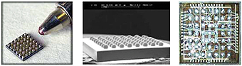
individual units in packages after dicing them from a wafer. This process is an extension of the wafer Fab processes, where the device interconnects and protection are accomplished using the traditional fab processes and tools. In the final form, the device is a die with an array pattern of bumps or solder balls attached at an I/O pitch that is compatible with traditional circuit board assembly processes. WLCSP is a true chip-scale packaging (CSP) technology, since the resulting package is of the same size of the die (Figure 1). WLCSP technology differs from other ball-grid array (BGA) and laminate-based CSPs in that no bond wires or interposer connections are required. The key advantages of the WLCSP is the die to PCB inductance is minimized, reduced package size, and enhanced thermal conduction characteristics.
Typical WLCSP Configurations and Dimensions
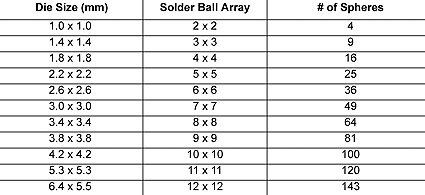
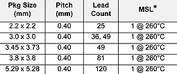
Available WLCSP packages from Freescale range from 2.0 × 2.0 mm to 5.29 × 5.28 mm in size, with a standard pitch of 0.40mm and a standard solder ball diameter of 0.250mm. The physical outlines of WLCSP packages are dynamic since those depend on actual die size. Therefore, users of devices in these packages must exercise greater care in utilization than with more standardized packages. Refer to Table 1 for details regarding die sizes for standard solder ball arrays at 0.40mm pitch, which complies to JEDEC Publication 95, Design Guide 4.18 [1] and JEDEC Standard MO-211. [2]
The PCB layout and stencil designs are critical to ensure sufficient solder coverage between the package and the Printed Circuit Board (PCB). When designing the PCB layout, refer to the Freescale case outline drawing to obtain the package dimensions and tolerances.
WLCSP Construction
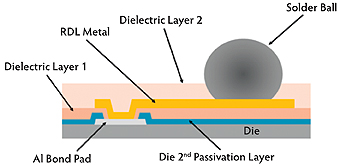
Refer to Figure 2 for a representation of a typical WLCSP package with a RDL layer between two dielectric layers. A WLCSP die has a first layer of dielectric, a Copper metal redistribution layer (RDL) to re-route the signal path from the die peripheral to a solder ball pad, and a second dielectric layer to cover the RDL metal, which in turn is patterned into the solder ball array. The solder ball is a lead-free alloy.
Process Flow
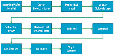
A typical WLCSP process flow is illustrated Figure 3. The illustration displays the process for a two-layer RDL process, with the RDL metal layer between two dielectric layers.
Printed Circuit Board (PCB) Level Guidelines
PCB Design Guideline
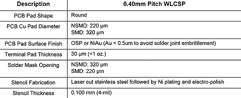
PCB design requirements are based on IPC-A-600 [3] standards. For optimum electrical performance and highly reliable solder joints, Freescale recommends the PCB and stencil design guidelines listed in Table 2.
PCB Land Design Guidelines
Solder Mask Defined (SMD) pads are defined by the solder mask opening on the board pad as shown in Figure 4. The opening of the solder mask is smaller than the
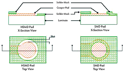
underlying copper area for soldering to the associated bump. A Non-Solder Mask Defined (NSMD) pad has a solder mask opening larger than the copper pad. There are many factors influencing whether the PCB designer uses SMD or NSMD pads. Either type can successfully be used with WLCSP packages. Freescale recommends using NSMD pads for thermal fatigue and SMD pads for drop test performance. Fillets where the trace connects to the Cu pad are recommended, especially with NSMD pads.
Via-In-Pad Structures
The need for via-in-pad structures will generally be determined by the design. Via-in-pad designs typically result in voids and inconsistent solder joints after reflow, leading to early failures. These voids are due to trapped air in the via. If via-in-pad structures must be used, it is recommended to use filled vias. As with any PCB, the quality and experience of the vendor is very important with via-in-pad designs.
Stencil Design Guideline
Due to the fine pitch and small terminal geometry used on WLCSP, particular attention must be paid to the paste printing process. In process inspection for paste height, percent pad coverage, and registration accuracy to solderable land patterns is highly recommended.
Solder Stencil Design and Fabrication
Stencils should be laser cut stainless steel with Nickel plating or electroformed Cobalt or Chromium hardened Nickel for repeatable solder paste deposition from ultra small apertures required by small pitch packages. It is recommended to inspect the stencil openings for burrs and other quality issues prior to use. Both square and round shaped apertures have been used successfully, however square shaped aperture openings provide more consistent paste printing and transfer efficiency when compared to round openings. Corners may be rounded to prevent clogging. 1:1 aperture to pad ratio is recommended for SnAgCu alloys.
For 0.40mm pitch WLCSP devices, use aperture aspect ratio of > = 0.66, with 0.25mm × 0.25mm square openings (25 micron corner radius) for improved solder paste deposition repeatability. Aperture aspect ratio is defined as the aperture opening area divided by the aperture side wall surface area.
A 0.100mm (4-mil) thick stainless steel stencil is recommended. When these stencil design requirements conflict with other required SMT components in a mixed technology PCB assembly, a step-down stencil process may be utilized in compliance with IPC-7525 [4] design standards.
PCB Assembly
Assembly Process Flow
A typical Surface Mount Technology (SMT) process flow is depicted in Figure 5.

WLCSP PCB Assembly Guideline
Screen Printing: Solder Paste Material
Use of Type 4 (25 to 36 micron solder sphere particle size) or finer solder paste is recommended and a low halide (< 100ppm halides) No-Clean rosin/resin flux system be used to eliminate post-reflow assembly cleaning operations.
Component Placement
The WLCSP package is comparatively small in size. For better accuracy, it is recommended to use automated fine-pitch placement machines with vision alignment instead of chip-shooters to place the parts. Local fiducials are required on the board to support the vision systems.
Pick and Place systems using mechanical centering are not recommended due to the high potential for mechanical damage to the WLCSP device. Ensure minimal pick-and-place force is used to avoid damage, with all vertical compression forces controlled and monitored. Z-height control methods are recommended over force control. Freescale recommends the use of low-force nozzle options and compliant tip materials to further avoid any physical damage to the WLCSP device.
Use only vacuum pencil with compliant tip material whenever manual handling is required.
All assemblers of WLCSP components are encouraged to conduct placement accuracy studies to provide factual local knowledge about compensations needed for this package type. Freescale cannot anticipate the range of placement equipment and settings possible for package placement and therefore cannot make a generic recommendation on how to compensate for WLCSP interchangeability.
Reflow Soldering
Temperature profile is the most important control in reflow soldering and it must be fine tuned to establish a robust process. The actual profile depends on several factors, including complexity or products, oven type, solder type, temperature difference across the PCB, oven and thermocouple tolerances, etc. All of Freescale’s WLCSP devices are qualified at Moisture Sensitivity Level 1 at 260°C. The maximum temperature at the component body should not exceed this level. Actual reflow temperature settings need to be determined by the end-user, based on thermal loading effects and on solder paste vendor recommendations.
Rework Procedure
WLCSP components removed during PCB rework should not be reused for final assemblies. Freescale follows standard component level qualifications for packages/components and these include three solder reflows survivability. A package that has been attached to a PCB and then removed has seen two solder reflows and if the PCB is double sided, the package has seen three solder reflows. Thus the package is at or near the end of the tested and qualified range of known survivability. These removed WLCSP components should be properly disposed of so that they will not mix in with known good WLCSP components.
The rework process for WLCSP devices is similar for typical BGA and CSP packages:
• To remove the faulty component from the board, hot air should be applied from the top and bottom heaters. An air nozzle of correct size should be used to conduct the heat to the WLCSP component such that the vacuum pick up tool can properly remove the component. It is recommended to apply top and bottom heaters simultaneously for 30 seconds at 300°C and 150°C, respectively. Many assembly sites have extensive in-house knowledge on rework and their experts should be consulted for further guidance.
• Once the WLCSP component is removed, the site is cleaned and dressed to prepare for the new component placement. A de-soldering station can be used for solder dressing. It should be noted that the applied temperature should not be > 245°C, otherwise the copper pad on the PCB may peel off.
• A mini-stencil with the same stencil thickness, aperture opening and pattern as the normal stencil should be used. Apply a gel or tacky flux using a mini-metal squeegee blade. The printed pads should be inspected to ensure even and sufficient solder paste before component placement.
• A vacuum nozzle is used to pick the new package up, and accurately place it using a vision alignment placement tool. A split light system that displays images of both the WLCSP leads and the footprint on the PCB is recommended.
The replaced component is then soldered to the PCB using a temperature profile similar to the normal reflow soldering process.
Moisture Sensitivity Level Rating
The Moisture Sensitivity Level (MSL) indicates the floor life of the component and its storage conditions after the original container has been opened. The lower the
MSL value, the less care is needed to store the components. Table 3 depicts the best case MSL for each package size. All WLCSP devices at Freescale Semiconductor are MSL1, testing in accordance with IPC/JEDEC J-STD-020D. [5]
* Note: Please refer to Freescale Semiconductor web site for specific product MSL and package information, including JEDEC MSL.
Board Level Reliability
The board level reliability is usually presented in terms of solder joint life. The solder joint results in this section utilized the board layout guidelines from Section (PCB Design Guideline).
Testing Details
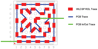
Samples of WLCSP in daisy chain format were used to study the solder joint reliability. BGA pairs were routed together in the WLCSP RDL layer, with a complementary pattern designed on the test PCB to provide one electrical circuit (net) through the package when the package is attached to the test PCB, as illustrated in Figure 6.
Solder Joint Reliability (SJR) Results
Assembled PCBs can be temperature cycled at a variety of temperature ranges. The most common test condition for small devices such as these at Freescale is JEDEC Condition ‘G’ [6] (-40°C/+125°C), with 15 minute dwell times for a typical frequency of one cycle per hour.
Freescale has the capability of continuously monitoring the resistance through a daisy chain package and its complementary test PCB. Failure is defined as resistance through the daisy chain net of 300 Ohms or greater. Daisy chain nets are tested (time zero testing) prior to temperature cycling.
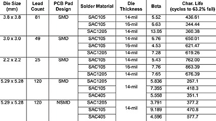
Freescale continues to work on understanding and improving the solder joint reliability of WLCSP packages. From the various experiments, the solder joint reliability performances for the different package size, lead count, die thickness, and solder material are shown in Table 4. All experiments were performed using similar size test boards.
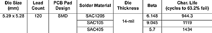
An alternate condition (0/100 °C) was also evaluated. This condition employed 10 min ramp and dwell times, providing 1.5 cycles per hour. Results for this condition are shown in Table 5.
Underfill
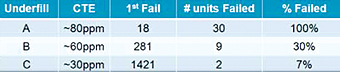
Data on underfill was collected on a 5.29 × 5.28mm die size with SAC1205 0.25mm diameter solder spheres. Careful selection of underfill material is critical for enhancing BLR performance of WLCSP packages. Selecting an underfill with too high a CTE can result in worse BLR performance than no underfill. Underfilling can significantly increase the solder joint reliability of WLCSP packages. A comparison of non-underfill vs underfilled results for a 5.29 × 5.28mm die size shows a 7X improvement in cycles to 1st failure (201 vs 1421).
Mechanical Drop Test
WLCSP parts were tested per JEDEC’s JESD22-B111 Drop Test Specification [7]. The drop test set-up, board layout, fixtures, and criteria are all based on the JESD22-B111. All drops are carried out in the -Z direction (package down). The peak acceleration is 1500g for 0.5 ms (half-sine pulse). The resistance at time zero and still state after the drop are recorded. Resistance data was collected in-situ throughout the dropping process, with maximum resistance data recorded during the drop. The failure criteria is 100 Ohms for 200 nano-seconds, recorded 3 times during 5 consecutive drops.
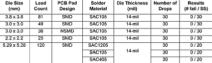
From the various experiments, the drop test performances for the different package sizes and lead counts are shown in Table 6.
Package Thermal Resistances
The thermal performance of WLCSP is characterized using two thermal board types and three boundary conditions:
Board Types:
1. Single Signal Layer – 1s (designed per JEDEC EIA / JESD51-3 [8].
2. Two Signal Layers, Two Internal Planes – 2s2p (designed per JEDEC EIA / JESD51-5 [9] and JEDEC EIA / JESD51-7 [10]
Thermal Resistance Boundary Conditions:
1. Junction-to Ambient (Theta-JA)
2. Junction-to-Board (Theta-JB)
3. Junction-to-Case (Theta-JC)
These thermal resistances help bound the thermal problem under distinct environments.
Junction-to Ambient (Theta-JA)
Junction-to-ambient thermal resistance (Theta-JA JEDEC EIA/JESD51-2 [11]) is a one-dimensional value that measures the conduction of heat from the junction (hottest temperature on die) to the environment near the package. The heat that is generated on the die surface reaches the immediate environment along two paths: (1) convection and radiation off the exposed surface of the package and (2) conduction into and through the test board followed by convection and radiation off the exposed board surfaces. Theta-JA is reported with two parameters, depending on the board type used: R JA and R JMA. R JA and R JMA help bound the thermal performance of the WLCSP package in a customer’s application.
• R JA measures the thermal performance of the package on a low conductivity test board (single signal layer – 1s) in a natural convection environment. The 1s test board is designed per JEDEC EIA/JESD51-3 and JEDEC EIA/JESD51-5. R JA helps estimate the thermal performance of the WLCSP when it is mounted in two distinct configurations: (1) a board with no internal thermal planes (i.e., low conductivity board) or (2) when a multi-layer board is tightly populated with similar components.
• R JMA measures the thermal performance of the package on a board with two signal layers and two internal planes (2s2p). The 2s2p test board is designed per JEDEC EIA/JESD51-5 and JEDEC EIA/JESD51-7. R JMA provides the thermal performance of the package when there are no nearby components dissipating significant amounts of heat on a multi-layer board.
Junction-to-Board (Theta-JB)
Junction-to-board thermal resistance (Theta-JB or R JB per JEDEC EIA/JESD51-8 [12]) is also provided for the WLCSP. R JB measures the horizontal spreading of heat between the junction and the board. The board temperature is taken 1 mm from the package on a board trace located on the top surface of the board.
Junction-to-Case (Theta-JC)
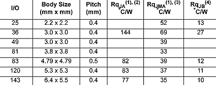
Another thermal resistance that is provided is junction-to-case thermal resistance (Theta-JC or R JC). The case is defined at the exposed pad surface. R JC can be used to estimate the thermal performance of the WLCSP package when the board is adhered to a metal housing or heat sink and a complete thermal analysis is done.
Table 7 has some thermal information for certain WLCSP packages [13]. All of the data was generated using Silicon (Si) die. There is an inverse relationship between the body size of the package and the thermal resistances. Large packages have lower R JMA values. The greater the body size the more PTH vias will fit under the package ■
Notes:
1. Junction temperature is a function of die size, on-chip power dissipation, package thermal resistance, mounting site (board) temperature, ambient temperature, power dissipation of other components on the board, and board thermal resistance.
2. JEDEC EIA/JESD51-2 with the single layer board horizontal. Board conforms to JEDEC EIA/JESD51-3 and JEDEC EIA/JESD51-5.
3. Per JEDEC JESD51-6 [14] with the board horizontal. Board conforms to JEDEC EIA/JESD51-5 and JEDEC EIA/JESD51-7.
4. Thermal resistance between the die and the printed circuit board per JEDEC EIA/JESD51-8. Board temperature is measured on the top surface of the board near the package.
References
[1] JEDEC Publication 95, Design Guide 4.18, Wafer Level Ball Grid Arrays (WLBGA), Issue. A, September, 20004.
[2] JEDEC MO211, “Die Size Ball Grid Array, Fine Pitch, Thin/Very Thin/Extremely Thin Profile”, June 2004.
[3] ANSI/IPC-A-600G, “Acceptability of Printed Boards”, July 2004.
[4] IPC-7525, “Stencil Design Guidelines”, May 2007.
[5] IPC/JEDEC J-STD-020D.1, “Moisture/Reflow Sensitivity Classification for Nonhermetic Solid State Surface Mount Devices”, May 2008.
[6] JEDEC JESD-A104C, “Temperature Cycling”, May 2005.
[7] JEDEC JESD-B111, “Board Level Drop Test Method of Components For Handheld Electronic Products”, July 2003.
[8] EIA/JESD51-3, “Low Effective Thermal Conductivity Test Board for Leaded Surface Mount Packages,” August 1996.
[9] EIA/JESD51-5, “Extension of Thermal Test Board Standards for Packages with Direct Thermal Attachment Mechanisms,” February 1999.
[10] EIA/JESD51-7, “High Effective Thermal Conductivity Test Board for Leaded Surface Mount Packages,” February 1999.
[11] EIA/JESD51-2, “Integrated Circuits Thermal Test Method Environment Conditions – Natural Convection (Still Air)”, December 1995.
[12] EIA/JESD51-8, “Integrated Circuit Thermal Test Method Environmental Conditions – Junction-to-Board”, October 1999.
[13] V. Chiriac, “Wafer Level CSP Thermal Performance Evaluation”, Freescale Semiconductor, August 2008.
[14] EIA/JESD 51-6, “Integrated Circuits Thermal Test Method Environment Conditions – Forced Convection (Moving Air),” March 1999.
www.freescale.com