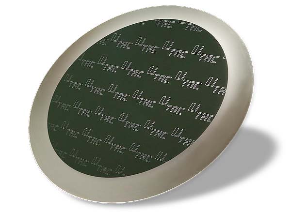
UTAC Holdings Ltd. (UTAC), a global semiconductor test and assembly services provider headquartered in Singapore, is further underlining its strength in advanced wafer process solutions. The company has added state-of-the-art plasma dicing and multi-project wafer (MPW) capabilities to its range of advanced semiconductor manufacturing solutions.
Plasma dicing allows narrow scribe street width between dies, resulting in the increase number of dies per wafer. It gives “near-perfect” dicing quality without any chipping and/or cracking and is a differentiated advantage over the conventional mechanical sawing process, which gives chronic sidewall quality issue.
Additionally, plasma dicing enables processing of different die in the same wafer. MPW allows sharing mask and wafer processes, thus enabling semiconductor companies to reduce overall cost and time-to-market by validating several designs using a single wafer. Qualification of new chips becomes much faster with shorter development cycle time. Additionally, with 100 percent die utilization, there is waste-free dicing. After dicing, the different MPW dies sizes can be reconstituted on separate wafer frames for shipment to the customers. This new capability enables UTAC to provide full turnkey MPW services.
UTAC’s plasma dicing capabilities can be extended to bumped solder ball and Cu pillar solutions as well as non-bumped wafers. There are no reliability issues for exposed AlCu pads, and no degradation of ball shear strength. UTAC can offer a pass reliability of THS 85C/85%RH at 1000 hours.
“I am very pleased to be one of the first OSAT’s to have successfully implemented plasma dicing in our Singapore facility”, says Dr. John Nelson, President and CEO at UTAC. “With my IDM background, I am well aware of the benefits of being able to increase the device quantity per wafer and more importantly the benefits of being able to dice multi-project wafers which can significantly shorten the cycle time of new product introduction”.
Earlier this year, UTAC acquired a wafer bumping facility in Singapore to complement its state-of-the-art WLCSP back-end processing capability on the island. The successful qualification and implementation of plasma dicing of wafers is another key milestone for UTAC’s advanced packaging capability.


