


 Toshiba Electronics Europe GmbH (“Toshiba”) introduces a new MOSFET gate driver IC TCK421G that controls the gate voltage of external N-channel MOSFETs based upon the input voltage.
The MOSFET gate driver is suitable for configuring a power multiplexer or a load switch circuit equipped with reverse-current blocking by being combined with a back-to-back connection of external N-channel MOSFETs.
The TCK421G incorporates a charge pump circuit that supports a wide range of input voltages (VIN) from 2.7 to 28.0V, providing a stable supply of 10V to the gate-source voltage of external MOSFETs thereby facilitating the switching of large currents. The typical input quiescent current in the ON state (IQ(ON)) is as low as 140mA while the standby current in the OFF state (IQ(OFF)) is just 0.5mA. In addition, the TCK421G contains an overvoltage and undervoltage lockout function. The gate drive voltage can be selected to suit the application.
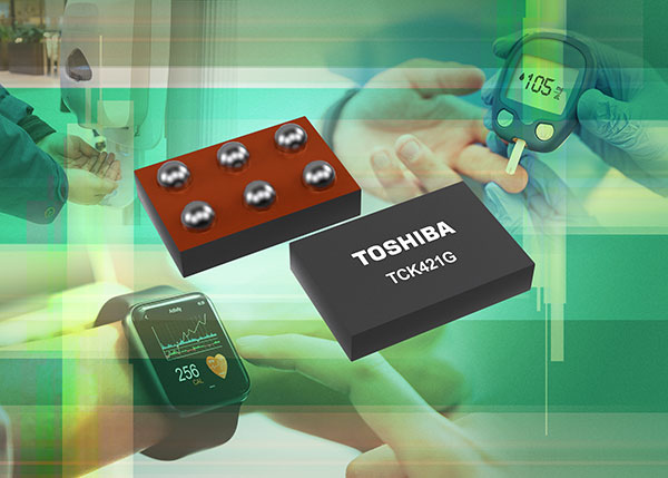
Housed in the chip scale WCSP6G package, the device has a footprint of just 1.2mm x 0.8mm and a height of 0.35mm. This is one of the smallest packages in the industry and allows use in densely packed devices such as wearables and smartphones.
The TCK421G is the first product launched in a series that will eventually comprise six devices. Due to its high efficiency and small size, the new driver can be used in a wide range of applications including battery powered, consumer and industrial equipment.
Shipment of the TCK421G starts today.