


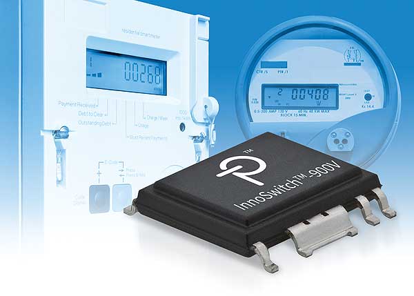
 When we look at the available switching power topologies there are many types that have evolved to suit specific requirements like higher power, improved efficiency, lower cost or reduced size but few can be considered revolutionary. The InnoSwitch™ family of power switching ICs from Power Integrations combine new technical innovations in power semiconductors that will revolutionise power supply design.
This new high voltage CV/CC flyback switching IC family features an integrated 900V power MOSFET, synchronous rectification and a precise secondary-side controller. Like all of the Inno-Switch families, the new InnoSwitch-EP ICs employ POWER INTEGRATIONS’ high speed magneto- inductive communication – termed FluxLink™, incorporated into the device package which creates a magnetic coupling between the primary and secondary side. FluxLink technology can provide very precise control of both of the primary and secondary switching functions, allowing synchronous rectification to be employed, delivering high efficiency without complex control circuitry (Figure 1).
Replacing the traditional Schottky diode with a MOSFET is the basis of synchronous rectification. MOSFETs have a very low on-resistance, RDS (ON), so the voltage drop across the transistor is much lower than for diodes, resulting in a significant increase in efficiency.
However, moving to synchronous rectification is not straightforward. Control circuitry is required to correctly phase the drive for the MOSFET on the primary side with that of the synchronous MOSFET on the secondary side. This control circuit must ensure that current only flows through one of the transistors at any given time.
To prevent overlap in the switching of the primary (flyback) and synchronous rectification MOSFETs (which would result in highly destructive cross conduction), controllers typically introduce a delay between the turn-off of one transistor and the turn-on of the other.
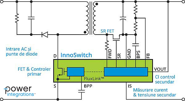
Figure 1
This “dead-time” must be sufficient to account for the variable propagation delays associated with the circuitry necessary to drive transistors on opposite sides of the isolation barrier. Integration of key switching elements (controller, MOSFETs and drivers) reduces this uncertainty and allows the dead-time to be reduced with a corresponding increase in efficiency.
So although synchronous rectification has advantages, it can be difficult to implement because the timing of the MOSFET’s switching is challenging.
The ideal approach is to control the primary-side switch from the secondary-side of the power supply. This avoids the need to predict of the state of either MOSFET allowing greatly reduced deadtime whilst ensuring that the two MOSFETs are never simultaneously in the on-state. However, until recently, synchronous rectification required additional external optocoupler circuitry, limiting the utility of synchronous rectification in compact and/or high-reliability applications.
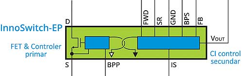
Figure 2
The FluxLink technology (figure 2) within InnoSwitch ICs eliminates the need for this extra circuitry. Precise control ensures that the dead time is neither too conservative – which would adversely affect efficiency – nor too aggressive which would risk the damaging effects of shoot-through.
As well as increasing efficiency, InnoSwitch-EP CV/CC flyback switching ICs enable excellent multi- output cross-regulation, and provide line protection and very fast transient response. Industrial applications increasingly require robust, reliable power supplies that provide long life and uninterrupted service reducing down time and service costs.
Multiple regulated outputs are often required to drive different functions that need power – clocks, motors, network interfaces, microprocessors, etc. Some functions require very tight voltage limits and to meet this engineers have previously used post-regulators that reduced efficiency and added cost to the solution.
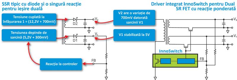
Figure 3
The forward voltage drop of a Schottky diode is current dependent (due to the epitaxial parasitic resistance in the Schottky structure) causing forward voltage drop to increase with rising load current. A single loop controller can only directly regulate a single output and is therefore unable to compensate for this change across multiple rectification stages.
The circuit shown in the right hand side of the diagram (figure 3) – based on Inno Switch-EP – uses a synchronous rectification MOSFET which has a relatively small change in voltage drop across load. This reduces cross regulation effects on the other outputs. Output voltage regulation at light and no-load is also improved by synchronous rectification.
The MOSFET switch greatly reduces the peakcharging of the output capacitor that typically causes a significant increase in output voltage when output load is insufficient. These highly efficient power supply switchers are the ideal solution for engineers looking to address increasingly demanding Total Energy Cosumption (TEC) regulations with an easy-to-implement solution that improves power supply efficiency from standby to full load.
For example, InnoSwitch-EP ICs enable a 20W power supply to achieve 90% efficiency in a multi- output design, while reducing no load consumption to less than 20mW. Voltage regulation across line is highly accurate, better than ±3%, along with accurate controlled over-current protection also provided (Figure 4).

Figure 4
Robustness is improved by having an integrated 900V power MOSFET capable of withstanding the significant line voltage fluctuations found in motor control, grid monitoring, industrial metering and renewable energy applications.
Designs can be made that support both line-neutral and phase-to-phase voltages. The 900V devices provide a high margin of safety in 450VAC systems and continue to operate during voltage swells and surges.
The IC also integrates advanced protection and safety features including: primary sensed output OVP; output over-current protection; hysteretic thermal shutdown; and line voltage monitoring with programmable under-voltage and overvoltage protection.
Companies designing for worldwide markets can be sure that a single 900V InnoSwitch-EP design will function reliably in even the most challenging regional conditions.
The 900V InnoSwitch-EP is UL1577 and TUV (EN60950) safety-approved and EN61000-4-8 (100A/m) and EN61000-4-9 (1000A/m) compliant. InnoSwitch-EP based power supplies can also help enable electronic products to meet productspecific efficiency requirements mandated by the U.S. DOE, ENERGY STAR (R), European Commission (Ecodesign Directive for ErP and Code of Conduct), California Energy Commission and other agencies.
Due to the high efficiency the devices do not require a heatsink and the unique eSOP package allows 900V InnoSwitch-EP ICs to be positioned across the isolation barrier which would otherwise be dead-space on the board.
For more details your CODICO contact or Ivan Mitic will be happy to help you!
Contact:
Ivan Mitic – Tel: +43 1 86305 194
e-mail: ivan.mitic@codico.com
CODICO | www.codico.com | www.codico.com/shop
![]()