


Panasonic Electric Works offers a wide range of PhotoMOS relays for use in telecommunication, measurement, security devices and industrial control. Obviously the PhotoMOS relay differs from the conventional electromechanical relay, but it also distinguishes itself from other switching solutions that utilize optocouplers and semiconductors. This application note describes the construction of a PhotoMOS relay and hot it differs from other types of switching devices.
The construction of the PhotoMOS relay is illustrated by Figure 1. The input pins are connected to a light emitting diode. This LED is located on the upper part of the relay and if a current flows through it, it starts emitting infrared light.
Below the LED there is an array of solar cells integrated into an optoelectronic device, located at least 0.4 mm from the LED.
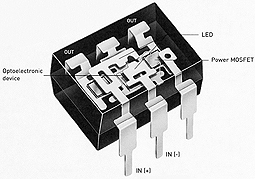
The light emitter and detector are moulded in a translucent resin that allows light to pass thus and provides a dielectric barrier between the input and output side. By integrating a resistor and a MOSFET in the optoelectronic device, it serves as a control circuit for switching the power MOSFETs and therefore the load circuit. These DMOS transistors are source coupled, thus providing bidirectional switching capabilities.
The connection of the parts can be easily illustrated by the schematic of the relay
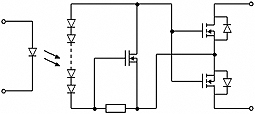
(Figure 2). If a current of about 3mA flows through the LED, it emits light.
The light is detected by solar cells and results in a voltage drop of about 10V across the array of cells. The driving circuit controls the photo voltage and thus the transistors switching the output.
By adding more solar cells to the optoelectronic device, the operating current of the relay can be further reduced, as far as 0.5mA.
By choosing different transistors for the output side, a whole range of relays can be offered.
Therefore we will take a closer look at the DMOSFET output transistor which significantly differs from standard MOSFETs used in integrated circuits. It has a vertical channel structure, source and drain are placed opposite the wafer as shown in Figure 3. As a result, more space for the source and drain region is available and the current rating can be increased.
During design of the DMOSFET the values of breakdown voltage, on-resistance, and the MOSFET’s capacities interact with each other. For example increasing the breakdown voltage up to 600 V requires a large and slightly doped drain area.
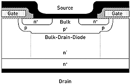
This will decrease capacities but increase on-resistance of the transistor to about 70Ω. If resistance is reduced to a few mΩ, changes of the drain area lead to higher transistor capacities and a lower breakdown voltage.
This interaction affects the relay’s characteristics in two ways:
1. During the switching operation the capacities of the DMOSFET have to be charged and discharged and thus influence the switching speed (20μs up to 5ms).
2. Since the on-resistance influences in max. power dissipation based on package type, the low load voltage types can carry a higher load current (60V/ 0.4A) and vice versa (600V/50mA).
Another important point for understanding the contact behaviour of the PhotoMOS relay is the DMOSFET’s intrinsic bulk-drain-diode in connection to drain and source. Thus a single transistor is only capable of switching a DC voltage since the diode will become forward biased if the polarity is reversed. Using a PhotoMOS relay for switching AC voltages requires two source coupled DMOSFETs.
By connecting the two output transistors of an AC relay in parallel, the allowable DC current can be increased up to 5A. Due to the behaviour of the DMOSFET and the resulting connection possibilities, relays for numerous applications are offered. Detailed information about the exact behaviour of a particular PhotoMOS relays can be obtained from its datasheet. Nevertheless, the advantages over electromechanical relays and other semiconductor solutions apply to all types of PhotoMOS:
• Low control current
• Controls small analog signals
• Low leakage current
• Stable on-resistance over lifetime
• Extremely long lifetime
• Small size
• No preferred position
• High vibration and shock resistance
• No bouncing and no switching noise
Due to the enormous variety of PhotoMOS relays, they are suitable for numerous applications. They can be used in telecommunication and measurement equipment, for switching and multiplexing I/O-signals, controlling small motors or power supplies, and for controlling various signals out of microcontrollers.
O’Boyle srl
Tel. +40 256-201346
Mail office@oboyle.ro
Web www.oboyle.ro