


Next-generation automotive technology trends represented by “CASE” (Connected, Autonomous, Shared, Electric) are driving higher expectations for automotive semiconductors. The demand for next-generation automotive microcontrollers (MCUs) with new functionality and more powerful operation-processing capabilities has necessitated a shift to a more advanced high-performance CMOS logic process in order to increase the scale and performance-power ratio of the integrated circuits (Figure 1). In addition, the control programs used on these next-generation MCUs are becoming larger in scale, demanding even faster instruction fetch speeds, which drives the need for larger capacity embedded flash memory with fast random-access read performance. For this reason, flash memory with high levels of performance and reliability that can be embedded alongside a more advanced high-performance CMOS logic process is a key technology in the development of next-generation automotive MCUs.
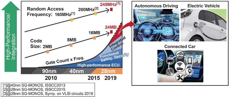
Figure 1: Trend Toward Higher Capacity and Faster Embedded Flash Memory in Automotive MCUs — (Source: Renesas Electronics Corp.)
At the same time, the introduction of over-the-air (OTA) software updates is proceeding alongside advances in connected car technology. This is creating strong demand for flash memory systems that can provide low-noise flash programming control to enable stable programming during software updates even while driving, a reduction in downtime when switching from the running software to a new version, and a robustness that is sufficient to prevent malfunctions even when an unexpected interruption occurs during updates or while switching software. To make OTA updates more convenient and easier to use, it is necessary to provide separate storage areas for program updates and currently running programs, which is driving further demand for larger flash memory capacities.
In response to the above requirements, Renesas Electronics Corporation (Renesas) has developed a new 28nm MCU embedded flash memory technology with the following features:
(1) 24 MB embedded flash memory – the industry’s largest in an MCU, combined with high-performance high-k metal gate (HKMG) CMOS logic circuits
(2) 240 MHz random access read speed – the industry’s fastest for embedded flash memory
(3) Support for low-noise programming during OTA updates
(4) Robust and high-speed software switching following OTA updates
Each of these items is described in detail below.
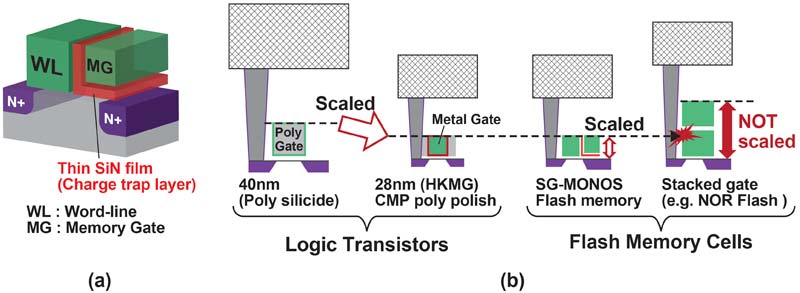
Figure 2: (a) Structure of SG-MONOS Flash Memory Cell, (b) Affinity with HKMG High-Speed CMOS Logic — (Source: Renesas Electronics Corp.)
24 MB Embedded Flash Memory – the Industry’s Largest in an MCU, Combined with High-Performance HKMG CMOS Logic Circuits
Renesas has used split-gate MONOS (SG-MONOS) technology combining excellent performance and reliability for embedded flash memory from the 150nm generation onward. Figure 2(a) illustrates the structure of a memory cell. In SG-MONOS flash memory, the stored electric charges are dispersed on the trap sites in the thin silicon nitride (SiN) film, which provides the two advantages.
First, defects in the insulator film have minimal impact on the retention of the stored charges, so it is possible to make the cells smaller without degrading reliability. Second, it is easier to make the height of the memory cells match with that of the logic transistors, which will allow flash memory cells to be added without changing the structure and performance of the logic transistors.
This advantage becomes particularly significant in cases where the height of the logic transistors decreases at the more advanced process nodes. Making full use of the above advantages, Renesas has developed the industry’s first automotive flash MCU with HKMG high-performance transistors in corporation with TSMC.
On the prototype chip, the memory cells have been shrunk to a size of less than 0.045 μm2, suppressing growth in the overall chip size while achieving 24 MB capacity of embedded flash memory for code storage (code flash: CF), the largest capacity in the industry. The chip also includes 1 MB of flash memory for data storage (data flash: DF) with a rated reprogramming cycle limit of 250,000 cycles.
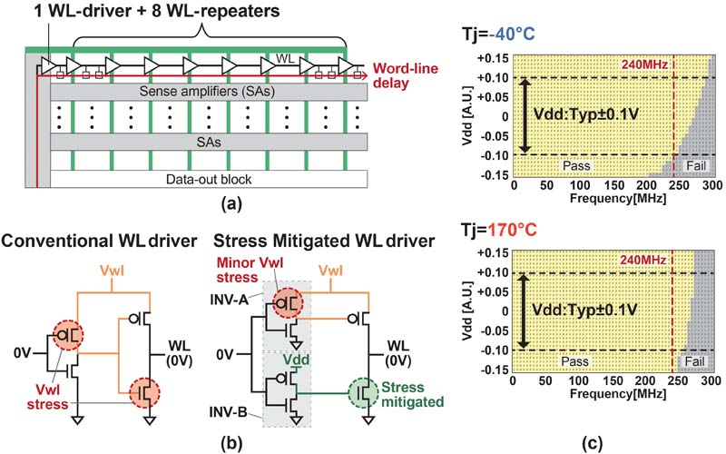
Figure 3: (a) Reduced WL Delay by WL Division, (b) WL Driver and Repeater Stress Voltage Mitigation, (c) Shmoo Plot of Random-Access Reads — (Source: Renesas Electronics Corp.)
240 MHz Random Access Read Speed – the Industry’s Fastest for Embedded Flash Memory
Word-line (WL) division, as shown in Figure 3(a), is an effective technique to speed up random access reads in flash memory. However, WL division increases the number of WL drivers and repeaters, which increases the area of the gate insulator film of the logic transistors to which the word line voltage (Vwl) are applied. This reduces reliability due to time-dependent dielectric breakdown (TDDB).
As shown in Figure 3(b), Renesas resolved this issue by changing the circuit structure of the WL drivers and repeaters, and providing a logic transistor power supply (Vdd), lower voltage than Vwl, as the drive voltage of the NMOS logic transistors at the final driver stage, which has the large gate insulator area. This made it possible to assure sufficient reliability by reducing the total area of the logic transistors to which Vwl is applied. Increasing the total channel width of the WL drivers and repeaters boosts the leak current and lowers Vwl at the end of the supply paths due to resistance along the Vwl lines, and this can degrade random-access performance. To resolve this, Renesas used a distributed Vwl drivers to minimize the effects of wiring resistance.
The above circuit techniques ensure reliability while realizing 240 MHz high-speed random-access read performance on the prototype chip – the industry’s highest read performance – over a wide temperature range (junction temperatures from −40°C to 170°C), as shown in Figure 3(c).
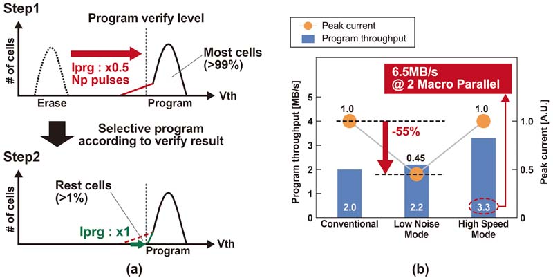
Figure 4: (a) Overview of Program Sequence that Varies the Write Current During Programming, (b) Comparison of Program Throughput and Peak Current Consumption among Write Modes — (Source: Renesas Electronics Corp.)
New Low-Noise Technology for Programming During OTA Updates
The charge pump circuit, which supplies the programming voltage, operates when the flash memory is programmed, generally resulting in large peak current consumption from the external power supply. If flash programming of an OTA update takes place in a high power-load environment, for example when the car is running and other circuits on the chip are operating, this peak current consumption could generate significant power supply noise, which would necessitate the addition of a large stabilizing capacitor. On the newly developed prototype chip, program operation is divided into two steps as shown in Figure 4(a).
The first step employs a low-noise mode in which the programming current (Iprg) flowing to the individual memory cells is reduced to half of the conventional programming current. Even when the programming current is halved, Vths of most memory cells (more than 99 percent) reach the desired level within the same programming time as with the conventional programming current. Then, the programming current – which is the same as the conventional program current – is applied only to the small remaining number of cells (less than 1 percent) that have not yet reached the desired level.
Thus, the overall programming current is reduced significantly. As shown in Figure 4(b), the new technology reduces the peak current consumption from the external power supply (Vcc) by 55 percent without reducing write throughput compared to the conventional programming condition.
Renesas has also applied the concept of varying the programming current in the implementation of a high-speed programming mode on the prototype chip.
This will reduce flash programming time required in factory programming on customers’ production lines and testing. In the first step of the programming operation, the programming current flowing through each of the memory cells is half that of the conventional approach and the number of cells to which programming voltage pulses are simultaneously applied is doubled, resulting in high-speed programming at 3.3 MB/s. When two macros are used in parallel, high-speed programming at 6.5 MB/s is possible.
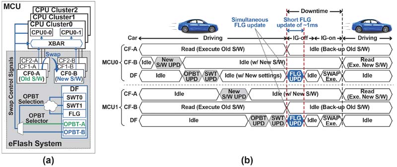
Figure 5: (a) Block Diagram of Prototype Chip, (b) Timing Chart of Control Software Updating and Switching — (Source: Renesas Electronics Corp.)
Robust and High-Speed Software Switching Following OTA Updates
Renesas has developed an embedded flash memory system suitable for OTA updates that is poised for rapid mainstream adoption in the near future. Figure 5(a) shows an overview of the CPU cluster block and flash memory system block of the prototype chip. To reduce downtime, the CF where the control software is stored is divided into two areas – a storage area for old software and a storage area for new software – and new software is saved in the background when the car is running. The prototype chip has three CPU clusters. Each CPU cluster (designated as CPU cluster n, where n = 0, 1, and 2) is connected via a cross-bar switch to CFn-A and CFn-B, each of which comprises a 4 MB CF macro. Making full use of the total 24 MB flash memory capacity, a control software storage area totaling 12 MB and a storage area for new software of equivalent size are provided for the three CPU clusters. To prevent malfunction after a software update or switching interrupt, multiplexing is provided for the software and setting information (OPBT), and history data and status flags (SWT0, SWT1, FLG, etc.) have been added. This ensures robust operation that allows executable control software to be selected reliably.

Figure 6: Photograph and Specifications of Prototype Chip — (Source: Renesas Electronics Corp.)
Figure 5(b) shows OTA operation when updating the control software of multiple MCUs installed in a single vehicle. Downtime can be reduced by first storing the new software in the individual MCUs while the car is running and then switching the flag information in all the MCUs when the ignition is turned off. The flag information update time is dominated by erase time. Fast erase of SG-MONOS cells by band-to-band tunneling (BTBT) contributes to fast FLAG update time of less than 1ms. This is so brief that it is perceived as there being no downtime at all.
Figure 6 shows a photograph and list of specifications of the prototype chip utilizing the new technologies described above. Flash memory macros and systems based on these newly developed technologies have been incorporated in the RH850/E2x and RH850/U2x Series MCUs, sample shipments of which have already begun.
Moving forward, Renesas is committed to the continued development of embedded flash memory and striving to achieve the higher capacities, higher speeds, and lower power consumption that will be required to support new applications.

About the Author
Yasuhiko Taito has been with Renesas Electronics Corporation working for embedded DRAM and Flash memory development for over 25 years. He is now in charge of the development of cutting edge embedded non-volatile memory for microcontroller units.
Renesas Electronics Corporation