


Lattice Semiconductor Corporation the leader in ultra-low power, small form factor, customizable solutions, announced the availability of the Functional Safety
Design Flow solution based on the Lattice Diamond® Design Tools. Certified by TÜV-Rheinland, an independent organization globally recognized for safety and quality testing, the package enables users to bring their product to market faster by simplifying and speeding up the IEC61508 safety certification process for applications using Lattice FPGAs.
“By using Lattice’s qualified Functional Safety Design Flow, designers can adhere to the latest safety design methodology when developing safety-critical designs, accelerate their certification process and reduce design costs”, said Jim Tavacoli, Sr. Director, Product and Segment Marketing, Lattice.
IEC61508 has become the global standard for functional safety certification, and many industry specific standards are derived from it. The Lattice solution comprises a design flow and the development tools necessary to ensure that applications comply up to Safety Integrity level 3 (SIL3) certification.
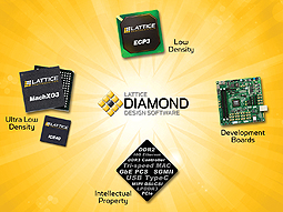
The Functional Safety Design Flow solution includes: Lattice Diamond Design Tools suite (a complete design and verification flow including Lattice Synthesis Engine and incorporating third party tools such as Aldec Active-HDL™ simulator and Synopsys Synplify Pro® synthesis) and Safety User Manual. Lattice FPGA families covered include both non-volatile (MachXO™, MachXO2™, LatticeXP2™) and SRAM-based (LatticeECP2™, LatticeECP2M™ & LatticeECP3™) products.
Lattice Semiconductor
www.latticesemi.com