


Designers are constantly looking for ways to architect their systems to provide an optimal computing solution that addresses all their application requirements. In many situations, that optimal solution often requires the use of field-programmable gate arrays (FPGAs), but many designers are woefully unfamiliar with the capabilities of these devices and how to go about incorporating them.
This article will briefly describe design scenarios that can benefit from the use of FPGAs. It will then go into the fundamentals of how they work before introducing some interesting FPGA solutions and development kits.
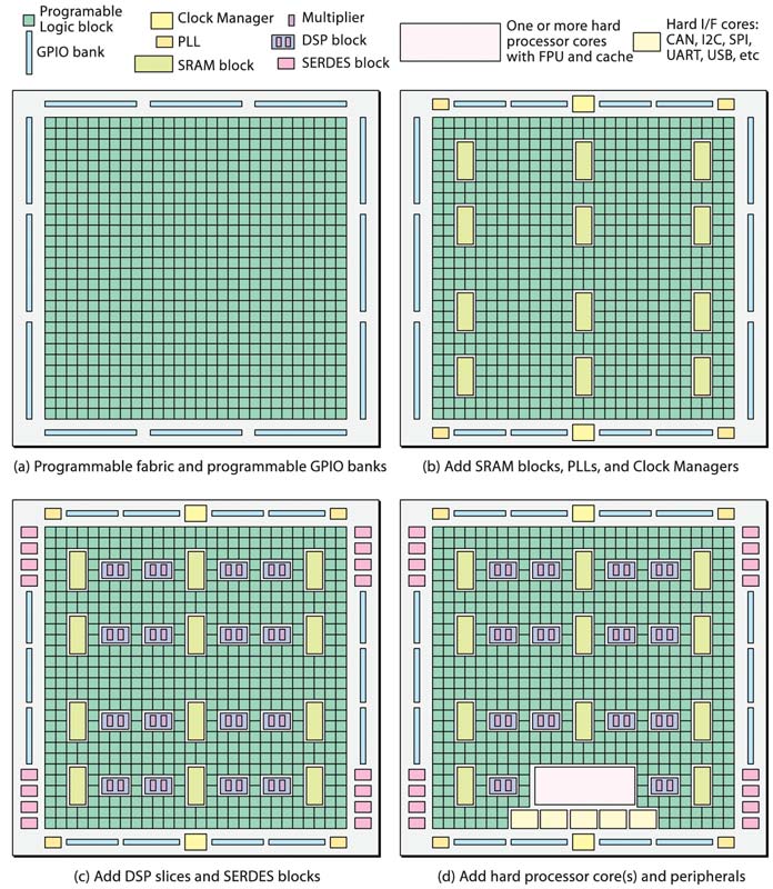
Figure 1: The simplest FPGAs contain only programmable fabric and configurable GPIOS (a), different architectures augment this fundamental fabric with SRAM blocks, PLLs, and clock managers (b), DSP blocks and SERDES interfaces (c), and hard processor cores and peripherals (d). — (Image source: Max Maxfield)
Why use FPGAs?
There are a wide range of computing applications, each of which may be best served by a different approach, including off-the-shelf microprocessors (MPUs) and microcontrollers (MCUs), off-the-shelf graphics processing units (GPUs), FPGAs, and custom system-on-chip (SoC) devices. Deciding which one to use requires a close look at the application requirements and considerations.
For example, when working on the cutting edge of technology like 5G base stations, designers need to consider that the underlying standards and protocols are still evolving. This means that designers need to be able to respond quickly and efficiently to any changes in specifications that are beyond their control.
Likewise, they need the flexibility to respond to future changes in standards and protocols that occur after the systems have been deployed in the field. Similarly, it is also necessary to be able to respond to unexpected bugs in system functionality or holes in system security, to modify existing functionality, or add new functionality in order to extend the life of the system.
While the highest performance is typically provided by an SoC, this route is expensive and time consuming. Furthermore, any algorithms that are implemented in the fabric of the chip are essentially “frozen in silicon.” This inherent inflexibility becomes a problem given the considerations outlined above. In order find the sweet spot of optimum performance and flexibility, an alternate route is required. That route is often provided by FPGAs, combinations of microprocessors/microcontrollers and FPGAs, or by FPGAs that boast hard processor cores as part of their fabric.
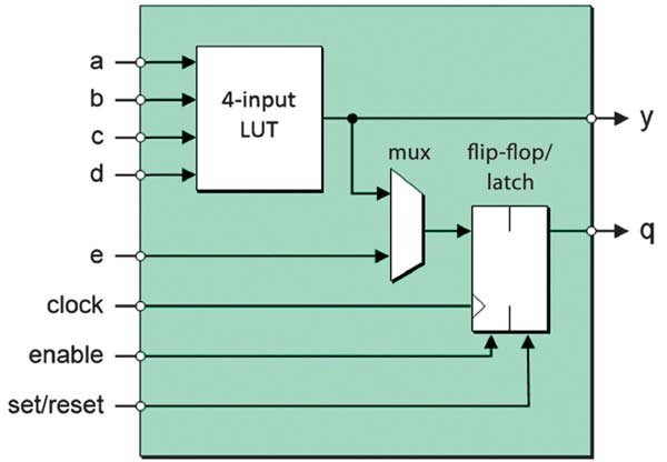
Figure 2: Each programmable logic block contains a collection of elements, including a look-up table, a multiplexer, and a register, all of which can be configured (programmed) to act as required. — (Image source: Max Maxfield)
What are FPGAs?
This is a tricky question because FPGAs are many things to many people. Also, there are many different types of FPGAs, each with different combinations of capabilities and functions.
At the heart of any FPGA – the defining aspect of “FPGA-dom,” as it were – is its programmable fabric, which is presented as an array of programmable logic blocks (Figure 1a). Each of these logic blocks contains a collection of elements – including a look-up table (LUT), a multiplexer, and a register – all of which can be configured (programmed) to act as required (Figure 2).
Many FPGAs use 4-input LUTs which can be configured to implement any 4-input logic function. In order to better support the wide data paths employed in some applications, some FPGAs offer 6, 7, or even 8-input LUTs. The output from the LUT is directly connected to one of the logic block outputs and to one of the multiplexer inputs. The other input to the multiplexer is directly connected to a logic block input (e). The multiplexer can be configured to select either of these inputs.
The output from the multiplexer feeds the register input. Each register can be configured to operate as an edge triggered flip-flop or a level sensitive latch (having said this, the use of asynchronous logic in the form of latches inside FPGAs is not recommended). Each register’s clock (or enable) can be configured to be active high or active low; similarly, the active level of the set/reset input(s) can also be configured.
These logic blocks can be thought of as “islands of programmable logic” floating in a “sea of programmable interconnect.” The interconnect can be configured to connect any output from any logic block to any inputs(s) of other logic block(s). Similarly, the primary inputs to the FPGA can be connected to the inputs of any logic blocks, and the outputs from any logic blocks can be used to drive the primary outputs from the device.
Regarding the primary general-purpose inputs/outputs (GPIOs), they are presented in banks (groups), where each bank can be configured to support a different interface standard such as LVCMOS, LVDS, LVTTL, HSTL, or SSTL. Additionally, the impedance of the inputs can be configured, as can the slew rate of the outputs.
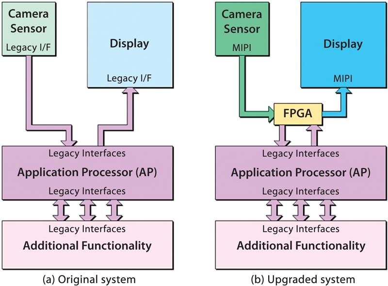
Figure 3: An FPGA can be used to provide an intelligent interface between other devices that use different interface standards or communications protocols, thereby extending the life of existing designs based on legacy devices. — (Image source: Max Maxfield)
The next step up the FPGA fabric includes things like blocks of SRAM, called block RAM (BRAM), phase lock loops (PLLs), and clock managers (Figure 1b). Digital signal processing (DSP) blocks (DSP slices) can also be added. These contain configurable multipliers and a configurable adder that allows them to perform multiply-accumulate (MAC) operations (Figure 1c).
Another common FPGA feature, high-speed SERDES blocks, can support gigabit serial interfaces. It’s important to note that not all FPGAs support all of the aforementioned features. Different FPGAs offer different collections of features targeted at different markets and applications.
The programmable fabric in an FPGA can be used to implement any logical function or collection of functions desired, all the way up to a processor core, or even multiple cores. If these cores are implemented in programmable fabric they are referred to as “soft cores”. By comparison, some FPGAs commonly referred to as SoC FPGAs, contain one or more “hard core” processors, which are implemented directly in the silicon (Figure 1d). These hard processor cores may include floating point units (FPUs) and L1/L2 cache.
Similarly, peripheral interface functions like CAN, I2C, SPI, UART, and USB can be implemented as soft cores in the programmable fabric, but many FPGAs include them as hard cores in the silicon. Communications between the processor cores, interface functions, and programmable fabric are typically realized using high-speed busses like AMBA and AXI.
The first FPGAs, which were presented to the market by Xilinx in 1985, contained only an 8 x 8 array of programmable logic blocks (no RAM blocks, DSP blocks, etc.). By comparison, today’s high-end FPGAs can contain hundreds of thousands of logic blocks, thousands of DSP blocks, and megabits of RAM. In total, they may contain billions of transistors equating to tens of millions of equivalent gates (e.g. 2-input NAND gates).
Alternative configuration technologies
The way in which the functions of the logic blocks and the routing of the interconnect is determined is by means of configuration cells, which may be visualized as 0/1 (off/on) switches. These cells are also used to configure the GPIOs interface standard, input impedance, output slew rate, etc.
Depending on the FPGA, these configuration cells may be implemented using one of three technologies:
• Antifuse: These configuration cells are one-time programmable (OTP), meaning that once the device has been programmed there is no going back. These devices tend to be limited to space and high security applications. Since they are sold in small quantities, their price tag is high, and they are an expensive design option.
• Flash: Like antifuse-based configuration cells, flash-based cells are nonvolatile. Unlike antifuse cells, flash cells can be reprogrammed as required. Flash configuration cells are tolerant to radiation, making these devices suitable for space applications (albeit with modifications to their upper metallization layers and packages).
• SRAM: In this case, the configuration data is stored in an external memory from where it is loaded each time the FPGA is powered up (or as commended in the case of dynamic configuration scenarios).
The advantages of FPGAs whose configuration cells are antifuse- or flash-based is that they are “instant-on” and they consume little power. One disadvantage of these technologies is that they require additional processing steps on top of the underlying CMOS process used to create the rest of the chip.
The advantage of FPGAs whose configuration cells are based on SRAM technology is that they are fabricated using the same CMOS process as the rest of the chip, and offer higher performance because they are typically one or two generations ahead of antifuse and flash technologies. The main disadvantages are that SRAM configuration cells consume more power than their antifuse and flash counterparts (at the same technology node), and they are susceptible to single event upsets (SEUs) caused by radiation.
For a long time, this latter point meant that SRAM-based FPGAs were considered unsuitable for aerospace and space applications. More recently, special mitigation strategies have been employed, with the result that SRAM-based FPGAs are found on systems like the Mars Curiosity Rover, alongside their flash-based cousins.
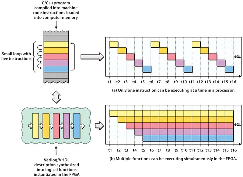
Figure 4: Unlike microprocessors in which only a single instruction can be executed at a time (sequentially), multiple functional blocks in an FPGA can execute at the same time (concurrently); also, FPGAs can implement appropriate algorithms in a massively parallel fashion. — (Image source: Max Maxfield)
Using FPGAs offers flexibility
FPGAs are used for many diverse applications. They are particularly useful for implementing intelligent interfacing functions, motor control, algorithmic acceleration and high-performance computing (HPC), image and video processing, machine vision, artificial intelligence (AI), machine learning (ML), deep learning (DL), radar, beamforming, base stations, and communications.
One simple example is to provide an intelligent interface between other devices that use different interface standards or communications protocols. Consider an existing system that contains an application processor connected to a camera sensor and a display device using legacy interfaces (Figure 3a).
Now assume that the creators of the system wish to upgrade the camera sensor and display device to something more modern that are lighter, cheaper, and consume less power. The only problem is that one or both of these new peripherals may use a modern interface standard that is not supported by the original application processor (AP). Alternatively, they may support a completely different communications protocol, like the Mobile Industry Processor Interface (MIPI). In this case, using an FPGA with its ability to support multiple I/O standards, coupled with some soft MIPI IP cores, will provide a fast, low-cost, risk-free upgrade path (Figure 3b).
As another application example, consider some compute-intensive task like performing the signal processing required to implement a radar system, or the beamforming in a communications base station.
Conventional processors with their von Neumann or Harvard architectures are well-suited to certain tasks, but they are less suited to ones that require the same sequence of operations to be performed repeatedly. This is because a single processor core running a single thread can only execute one instruction at a time (Figure 4a).
By comparison, multiple functions can be executing simultaneously in the FPGA, thereby allowing a series of operations to be pipelined, which in turn allows for much greater throughput. Similarly, rather than perform the same operation, say an additional 1,000 times on 1,000 pairs of data values with the processor, the same calculations could be performed in a massively parallel fashion in a single clock cycle in the FPGA by instantiating 1,000 adders in the programmable fabric (Figure 4b).
Who makes FPGAs?
This is an ever-evolving landscape. The two main manufacturers of really high-end devices with the highest capacity and performance are Intel (which acquired Altera) and Xilinx. The Intel and Xilinx offerings span the range from low-end FPGAs to high-end SoC FPGAs. Another vendor that focuses almost exclusively on FPGAs is Lattice Semiconductor, which targets low- and mid-range applications. Last but not least, Microchip Technology (via its acquisitions of Actel, Atmel, and Microsemi) now fields multiple families of small- to medium-sized FPGAs and low-end members of the SoC FPGA category.
Choosing the best device for the task at hand can be tricky because there are so many families, each offering different resources, performances, capacities, and packaging styles. Case in point, here are some examples: Intel devices; Lattice Semiconductor devices; and Xilinx devices.
How to design with FPGAs?
The traditional way to design FPGAs is for engineers to use a hardware description language like Verilog or VHDL to capture the design’s intent. These descriptions may first be simulated to verify they perform as required, after which they are passed to a synthesis tool that generates the configuration file used to configure (program) the FPGA.
Each FPGA vendor either has its own internally developed tool chain or offers a customized version of a tool from a specialist vendor. In either case, the tools can be accessed from the FPGA vendors’ websites; also, there may be free or low-cost versions of the full-blown tool suites.
In order to make FPGAs more accessible to software developers, some of the FPGA vendors now offer high-level synthesis (HLS) tools. These tools interpret an algorithmic description of desired behavior captured at a high level of abstraction in C, C++, or OpenCL, and generate the input to feed the lower-level synthesis engine.
For designers looking to get started, there are many development and evaluation boards available, each offering different capabilities and features. Three examples are the DFR0600 development kit from DFRobot which features a Zynq-7000 SoC FPGA from Xilinx, the DE10 Nano from Terasic Inc. which features a Cyclone V SoC FPGA from Intel, and the ICE40HX1K-STICK-EVN evaluation board which features a low-power iCE40 FPGA from Lattice Semiconductor. Designers planning on using an FPGA-based PCIe daughter card to accelerate applications running on an X86 motherboard may wish to look at something like one of the Alveo PCIe daughter cards, also from Xilinx.
Conclusion
Optimal design solutions are often provided by FPGAs, combinations of processors and FPGAs, or by FPGAs that boast hard processor cores as part of their fabric. FPGAs have evolved rapidly over the years and are able to address many design requirements in terms of flexibility, processing speed, and power, making them useful for a wide range of applications.
 Author: Rich Miron – Contributed by Digi-Key’s North American Editors
Rich Miron, Applications Engineer at Digi-Key Electronics, has been in the Technical Content group since 2007 with primary responsibility for writing and editing articles, blogs and Product Training Modules. Prior to Digi-Key, he tested and qualified instrumentation and control systems for nuclear submarines. Rich holds a degree in electrical and electronics engineering from North Dakota State University in Fargo, ND.
Digi-Key Electronics | https://www.digikey.com
![]()