


Extensive experience with ISM-RF products has revealed various pitfalls common to the layout of PCBs for these products. It’s not unusual to find significant variations in performance when the same IC is placed on two different circuit boards. Variations in the operating range, harmonic emissions, interference susceptibility, and start-up time serve to illustrate the role that layout can play in a successful design.
This article addresses various design oversights, explains why each error causes problems and recommends how to avoid these traps.
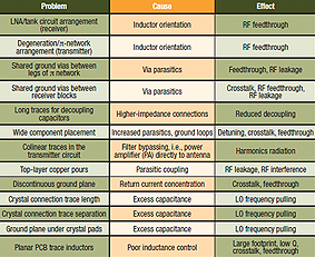
The table lists some possible PCB-layout problems, their causes and their effects. Most of these problems derive from one of a few common causes:
Inductor orientation
Mutual inductance is present when two inductors are in proximity. Current in the first circuit induces a magnetic field that stimulates current in the second circuit. When the two currents interact through the magnetic field, the resulting voltage is governed by the mutual inductance.
The best trade off between circuit compactness and reduced coupling is to properly orient inductors. You should orient the inductors orthogonally whenever possible. Consider, for example, the circuit board of an evaluation kit (MAX7042EVKIT) for a low-power FSK superheterodyne receiver. Because the three inductors on this board (L3, L1, and L2) are in proximity, they are oriented at 0°, 45°, and 90° to minimize mutual inductance.
Trace coupling
Individual traces can also affect coupling caused by magnetic fields if they are positioned too close together. This layout problem also creates mutual inductance. Of greatest concern in an RF circuit are those traces associated with sensitive parts of the system – such as the input matching network, the tank circuit in a receiver and the antenna-matching network in a transmitter.
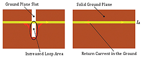
Routing a return current path close to the primary current path minimizes the radiated magnetic field. Such layouts reduce the area of the circuit loop. The ideal low-impedance path for return currents is usually a ground plane under the trace. A split ground (Figure 1), on the other hand, increases the loop area. For traces passing over the split, the return current is forced to follow a higher-impedance path that effectively increases the area of the current loop.
This layout also makes the trace more susceptible to the effects of mutual inductance. As with inductors, orientation of the traces plays a role in the coupling of magnetic fields.
If it becomes necessary to run traces from sensitive circuits close to each other, it is preferable to run them in orthogonal directions to reduce coupling.
If that cannot be achieved, consider using a guard trace.
Ground vias
The primary cause of RF-layout problems can usually be traced back to nonideal circuit properties, both in the circuit components and in their interconnections. Thin traces act as inductive wires, and a trace running over a copper plane or next to other traces forms a distributed capacitance with those structures. When it runs through a via, it tends to exhibit both inductive and capacitive properties. Via capacitance comes primarily from the coplanar copper of the via pad and the ground plane, which are separated by a relatively small clearance ring.
Secondary effects come from the cylindrical copper of the plated-through hole itself. The effect of parasitic capacitance is typically small, and usually causes only a slight degradation of signal edges in high-speed digital lines.
The largest parasitic impact from vias is simply the nonideal inductance exhibited by all interconnects. Parasitic inductance often has the greatest influence on bypass-capacitor connections.
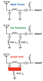
An ideal bypass capacitor provides a high-frequency short between power plane and ground plane, but nonideal vias reduce the low-inductance properties of both ground and power planes. Other problems arise when ground vias are shared between sensitive portions of a circuit, such as the two legs of a π network.
If you replace an ideal via with an equivalent lumped element inductor, the resulting schematic looks much different than intended (Figure 2).
Like the crosstalk from shared current paths, the resulting increase in shared mutual inductance can greatly amplify crosstalk and feedthrough.
Trace lengths
Data sheets for Maxim ISM-RF products often recommend that the high-frequency input and output lines be kept as short as possible to minimize loss and radiation. Such loss is typically due to nonideal parasitic properties of the interconnections.
Parasitic inductance and capacitance can both influence these circuit layouts, and are best avoided by using short trace lengths.
Ground planes and copper pours
A ground or power plane defines a common reference voltage and provides that voltage to all parts of the system through a low-impedance connection. In doing so, the plane equalizes any electric fields and thus acts as a good shielding mechanism. DC currents always follow the path of least resistance. Similarly, high-frequency currents always follow the path of least impedance. Therefore, for a standard PCB microstrip trace over a ground plane, the return current tries to flow in the area of ground plane just below the trace itself. Copper pours, also called guard traces, are used where a continuous ground is difficult to implement or where you need to shield sensitive parts of a circuit (Figure 3).
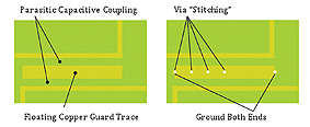
You can increase the shielding effect of a copper pour by tying the trace to ground at both ends and at multiple locations along its length. Use caution not to mix guard traces with traces intentionally designed to provide return currents, because that arrangement can cause unwanted crosstalk.
Not grounding a copper pour at all or tying it to ground at only one end can have limited benefit. By changing the impedance of nearby traces or acting as an unwanted “sneak” path between portions of a circuit, it can create parasitic capacitance that can have a detrimental effect.
These copper areas should be avoided, because they can interfere with the schematic design. Be sure to consider the effect of any ground plane near an antenna. Any monopole antenna will regard ground planes, traces, and vias as parts of the counterpoise, and nonideal counterpoise shapes can influence the antenna’s radiation efficiency and directionality. A ground plane, therefore, should not be placed directly under a monopole PCB trace antenna.
Excessive crystal capacitance
Parasitic capacitance can pull the operating frequency of a crystal oscillator off target.
Therefore, follow general guidelines to reduce any stray capacitance on the crystal leads, the solder pads, the traces, or the connection to the RF device.
Planar trace inductors
Use of planar trace or PCB spiral inductors is strongly discouraged. The inaccuracies inherent in a typical PCB-manufacturing process, such as the width and space tolerances, can greatly affect accuracy of the component value.
As a rule, the most controlled and highest-Q inductors are the wirewound variety.
Next are the ceramic-layer inductors. Nevertheless, some designers must use a spiral trace inductor as a last resort. The reasons to avoid this form of inductor are numerous. They are typically limited to low-inductance values due to space constrains, but the most critical reason is that their small geometry and poor control of critical dimensions often results in an unpredictable inductance value.
Conclusion
A few common PCB-layout traps can create problems in an ISM-RF design. You can avoid many of these pitfalls, however, with careful attention to the circuit’s nonideal properties. Following the guidelines above, you can save significant time and money that might otherwise be wasted on correcting mistakes.
A much more detailed version of this article including the equations required to calculate nonideal properties can be found at the Element14 web page: www.element-14.com/techfirst
The article has been provided by Farnell in cooperation with Maxim.
www.farnell.com