
As microcontroller applications get more complex, developers are using more Flash program memory for the application firmware. This is especially true with Internet of Things (IoT) endpoints that are starting to perform relatively complex edge computing. However, sometimes applications can expand to the degree that external program memory is required, at which point developers need to choose between parallel or serial Flash.
Adding an external parallel Flash memory chip ties up I/O lines, adds complexity, and consumes extra board space. This article will describe how to expand a microcontroller’s Flash program memory by adding an external serial Flash memory chip from Adesto Technologies that supports an SPI eXecute in Place (XiP) interface. It will also explain how XiP Flash is mapped into the memory space of a Microchip Technology microcontroller so that code execution is almost transparent to firmware.
Reasons for external memory expansion
Where possible, developers should start application development by selecting a microcontroller that has a roadmap of pin-compatible devices with more memory. If during development the application firmware expands to exceed the Flash memory on the target device, a pin-compatible device with more Flash can be easily substituted during development. This allows the application memory to expand without having to redesign the pc board for a different microcontroller.
However, the application may require more program memory than is available on-chip for a pin-compatible microcontroller family, requiring the use of off-chip Flash memory. This is becoming more common and can happen for a number of reasons, including:
• The system scope can expand past its initial concept during the development phase. This can be due to last-minute changes in the application, feature creep, or not accurately predicting the memory needs of the application. The options are to either upgrade with a pin-compatible microcontroller that has more Flash program memory, or add additional external Flash program memory which can delay the project if the development is already advanced.
• Future firmware upgrades in the field can require more Flash program memory than is available on the microcontroller already in the system board. In this situation the options are limited: either replace the systems in the field with ones containing more Flash program memory or cancel the upgrade.
• The system product family development might require a new product that needs more Flash program memory than is already available for the pin-compatible
microcontroller family. The options are to redesign the system using a new microcontroller family or add external Flash program memory.
Clearly, it is important for a developer to anticipate the needs of present and future systems for this memory expansion, and plan for it. If there’s a possibility the project will need external Flash program memory, the developer should lay out a place for future expansion of the pc board. While the Flash memory chip does not need to be populated on the board, it’s better to be safe and have the space already laid out.
The traditional way of expanding Flash program memory has been to use a parallel Flash interface with address and data lines. However, even the most efficient use of parallel Flash memory that does not sacrifice speed can use 16 bits of address, 16 bits of data, and four or more control signals. This requires 36 or more microcontroller pins.
Along with being an inefficient use of a microcontroller’s resources, this limits the microcontroller selection to devices with an external bus, which increases the microcontroller pin count. An external parallel bus also consumes significant pc board space, while the high speed address and data bus increase the possibility of electromagnetic interference (EMI).
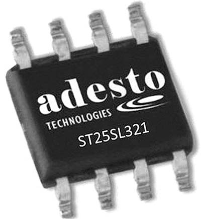
Figure 1: The Adesto AT25SL321 is a 32 Mbit Flash memory that supports single, dual, and quad SPI modes. It provides 32 Mbits of Flash memory in an 8-pin SOIC, DFN8, or TSSOP8 package. — (Image source: Adesto Technologies)
SPI XiP code execution
A more effective option is to use an external Flash program memory device that supports an SPI XiP interface. An SPI XiP interface can use only six pins to interface to the host microcontroller.
Unlike a conventional SPI interface, the memory on the external Flash memory device is not directly accessed with an SPI firmware driver, but is mapped in the microcontroller’s program memory.
A good example of a serial Flash memory device designed to interface using an SPI XiP interface is the AT25SL321-UUE-T from Adesto Technologies (Figure 1). This is a 32 megabit (Mbit) Flash memory that supports single, dual, and quad SPI modes. It supports an SPI clock of 104 megahertz (MHz), which in dual SPI mode provides an equivalent clock rate of 266 MHz, and in quad SPI mode an equivalent clock rate of 532 MHz.
Along with the 32 Mbits of Flash, the device has status registers to configure the device. Reading from the status registers can tell firmware if the device has a write or erase operation in progress. Writing to status registers allows blocks of Flash memory to be write protected.
The Adesto AT25SL321 also has 4 kilobits (Kbits) of one-time programmable (OTP) memory that can be used to store security information such as a unique serial number. It comes in an 8-pin SOIC, DFN8, or TSSOP8 package.
Like all serial memory devices that support SPI XiP, the Adesto AT25SL321 is configured using an instruction set specific to Adesto devices. The instruction set consists of 38 commands that are used by the host microcontroller to control the serial Flash. An SPI XiP peripheral on a host microcontroller will include a programmable state machine that is initialized on microcontroller power-up with the instruction set of the target serial Flash. Once initialized, the operation of the SPI peripheral is transparent to firmware executing code in the memory mapped SPI XiP region.
For example, if the host microcontroller firmware reads data from the memory mapped region, the SPI XiP that is configured with the Adesto instruction set sends a Read Data instruction code followed by a 24-bit byte address to the Adesto serial memory. The Adesto serial memory then sends the memory contents to the host microcontroller one byte at a time. To the firmware this appears as a normal read from memory.
Besides an SPI clock, data, and chip select pins, the Adesto AT25SL321 has two additional pins for enhanced in-system functionality. WP is an active-low write protect pin that prevents writing to the status register to write protect blocks of code. The microcontroller can use this pin to prevent low priority tasks from making unauthorized changes. HOLD is used to pause a data transfer in progress. This can be useful if the microcontroller receives a high priority interrupt signal while a data transfer to the memory is in progress and it needs to be paused until the interrupt is serviced.
The Adesto AT25SL321 32 Mbit Flash device supports four modes of operation:
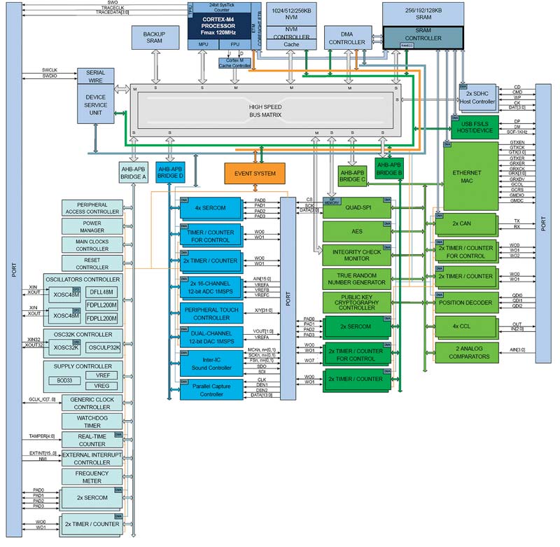
Figure 2: The Microchip ATSAMD51J20A has a full set of peripherals, including an SPI XiP serial interface, ADC, DAC, and support for data encryption. — (Image source: Microchip technology)
• Standard SPI operation: The Flash memory is accessed like a standard SPI memory device with SPI clock (SCLK), active-low chip select (CS), serial input (SI) data and serial output (SO) data. Standard SPI bus modes 0 and 3 are supported.
• Dual SPI operation: This provides twice the data rate of standard SPI operation by using SI and SO as bidirectional data pins, designated IO0 and IO1.
• Quad SPI operation: This provides four times the data rate of standard SPI operation. Besides IO0 and IO1, WP and HOLD are used as bidirectional data pins, IO2 and IO3. In quad SPI operation, WP and HOLD features are not available.
• QPI operation: This is only used for SPI XiP operation. While standard, dual, and quad SPI modes all support sending commands to the SPI memory using only the IO0 pin, QPI operation supports sending commands using the four IO[0:3] pins, significantly improving SPI XiP performance.
If the Adesto AT25SL321’s 32 Mbits are not sufficient, Adesto also offers the 64 Mbit AT25QL641-UUE-T. The two devices are pin compatible so the AT25QL641 can be a drop-in replacement. Besides having more memory, the only difference between the two devices is that the AT25QL641 is set to QPI operation by default on power-up. This reduces the setup time for the device in high performance systems. Both devices draw only 5 milliamps (mA) during a memory read cycle. Both Adesto memory devices operate off a single 1.7 to 2.0 volt rail and can interface to any voltage compatible microcontroller that has an SPI XiP interface.
For the host microcontroller, Microchip Technology has SPI XiP interfaces on its ATSAMD51 series, including the 120 MHz Arm® Cortex®-M4F-based ATSAMD51J20A-UUT microcontroller. This device has 1 Mbyte of Flash and 256 kilobytes (Kbytes) of RAM. It has a full range of peripherals including an analog-to-digital converter (ADC), digital-to-analog converter (DAC), USB port, and I2S. It also has a public key encryption peripheral and a true random number generator (TRNG) for security functions.
To connect to external Flash memory, developers can use the ATSAMD51J20A’s QSPI peripheral that supports SPI XiP. This allows code to be executed directly from the Adesto Flash memory. The ATSAMD51J20A maps the Adesto Flash into Arm’s Advanced High-Performance Bus (AHB) program memory space. To protect data in the serial Flash, the ATSAMD51J20A SIP XiP supports transparent scrambling of data written to external SPI memory and unscrambling of data read from external SPI memory. This can help prevent unauthorized firmware copying and system pirating.
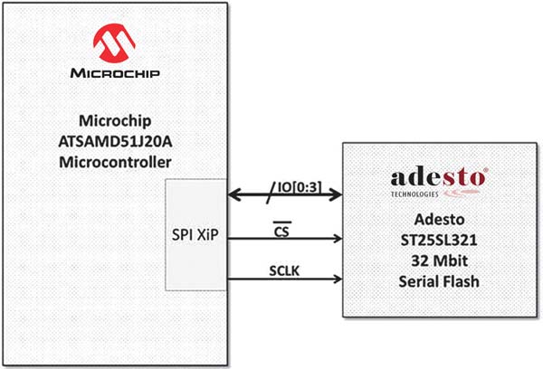
Figure 3: The Microchip ATSAMD51J20A 32-bit microcontroller has a QSPI peripheral that supports an SPI XiP serial port. This can interface easily to the Adesto AT25SL321 serial Flash using only six pins. — (Image source: Digi-Key Electronics)
Using the Microchip ATSAMD51J20A with an Adesto serial Flash memory device
The Microchip ATSAMD51J20A SPI XiP peripheral has three registers used to send commands to an external serial XiP Flash. Since the serial Flash XiP memory devices from different suppliers use different instruction codes, these registers must be configured as follows by the developer for the specific memory supplier used:
1. The Instruction Code Register contains the instruction used to access the serial Flash. For an Adesto Flash memory device operating in quad SPI mode, this register contains a Fast Read Quad Output instruction 0x6B if firmware is executing code out of the memory mapped XiP region. This register must be changed to the appropriate instruction code if a write, erase, or status register operation is being performed.
2. The Instruction Address Register contains the Flash memory address being accessed in the external serial Flash. When the Microchip ATSAMD51J20A SPI XiP is configured for serial memory mode, this address is automatically set by the SPI XiP peripheral to the address being executed by firmware in the memory mapped AHB memory space range 0x0400 0000 to 0x0500 0000.
3. The Instruction Frame Register configures the SPI XiP for the instruction frame format specific to the external memory device being used. This includes selecting the address length of 24 or 32 bits, enabling double-data rate (DDR), whether continuous read mode is supported, and the opcode length.
The rest of the Microchip SPI XiP interface is easily configured using the Microchip SPI drivers.
As long as the application firmware on the microcontroller is executing code out of the SPI XiP memory mapped region, the SPI XiP peripheral on the microcontroller does not need to be reconfigured. The Adesto Flash memory also supports a read mode with only the single SI pin with instruction code 0x03. If only dual SPI mode is being used, the instruction code is 0x3B. These codes are written by application firmware to the instruction code register.
It is considered good practice to flush any caches associated with memory mapped address space when the instruction code register is changed. When reading or writing to the serial Flash memory status registers, the cache should be flushed, then disabled. This should also be done when writing to the Flash in the memory mapped regions. The cache should be re-enabled once memory read operations are resumed.
Because of the high-speed data transfers involved, the serial Flash should be laid out on the pc board as close as possible to the microcontroller SPI XiP port. If that is not possible, then no trace should be longer than 120 millimeters (mm). The clock signal should be at least three times the width of the pc board traces away from other signals to avoid interference. The IO[0:3] bidirectional data signals should all be within 10 mm of each other to avoid skew.
Conclusion
External serial Flash memory devices can provide fast firmware code execution without the complexity and excess board space of parallel Flash chips. This allows for easy program code expansion over time, as well as field updates without redesigning the system board.

Author: Rich Miron – Applications Engineer at Digi-Key Electronics
Rich Miron, has been in the Technical Content group since 2007 with primary responsibility for writing and editing articles, blogs and Product Training Modules. Prior to Digi-Key, he tested and qualified instrumentation and control systems for nuclear submarines. Rich holds a degree in electrical and electronics engineering from North Dakota State University in Fargo, ND.
Digi-Key Electronics | https://www.digikey.com
![]()