


 What is an analog-to-digital converter driver and why do I need one?
As the name implies, analog-to-digital converter (ADC) drivers are specialty amplifiers that are designed specifically to work alongside ADCs, including successive approximation, pipelined and delta-sigma based architectures. These specialty amplifiers are critical circuit components that enable the ADC to function at full performance, as will be explored in the next sections. The need for analog signal conditioning, including ADCs, continues to grow as sensors become more and more abundant within a variety of end markets. These end markets include:
- Communications
- Medical
- Consumer
- Industrial
- Automotive
For ADCs, the market trend is toward higher resolution and higher speed devices as the cost of such solutions becomes more affordable.
Understanding ADC Inputs
Before discussing the technical functions required from an ADC driver, a brief overview of the input architecture of today’s ADC is needed. A differential signal can be defined as two nodes that have equal but opposite signals around a fixed point (the common mode level). The two signal nodes are typically referred to as positive and negative (non-inverting and inverting), as shown in Figure 1.
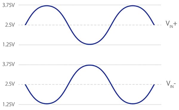
Figure 1: Differential sine wave example (© Microchip Technology)
In the above example, the full-scale input voltage is 5V peak-to-peak differentially, with each leg swinging 2.5V peak-to-peak. The common mode level in this example is 2.5V. A majority of today’s higher performance ADCs implement a differential input architecture, as it provides superior performance (relative to single-ended inputs). These performance benefits include the ability to reject common mode noise and common interference signals and a 6 dB (or a factor of 2) increase in dynamic range.
ADCs can pose an especially difficult challenge to system designers, offering a variety of different input sampling architectures that must be considered on the system level. For the purposes of this discussion, the focus will be on ADCs that use a switched-capacitor structure to accomplish input sampling. In its most basic form, this input structure is composed of a relatively small capacitor and an analog switch, as shown in Figure 2 below.
When the switch is configured in position 1, the sampling capacitor is charged to the voltage of the sampling node, in this case VS. The switch is then flipped to position 2, where the accumulated charge on the sampling capacitor is then transferred to the rest of the sampling circuitry. The process then begins all over again.
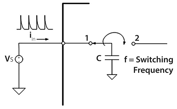
Figure 2: Simple switched-capacitor input structure (© Microchip Technology)
An unbuffered switched-capacitor input, like the one described above, can cause significant system level issues. The current required to charge the sampling capacitor to the appropriate voltage must be supplied from the external circuitry connected to the ADC input. When the capacitor is switched to the sampling node (switch position 1 in Figure 2), a large amount of current will be required to begin charging the capacitor. The magnitude of this instantaneous current is a function of the size of the sampling capacitor, the frequency at which the capacitor is switched, and the voltage present on the sampling node. This switching current can be described by the following equation:
iin = CVf
In the example above, C is the capacitance of the sampling capacitor, V is the voltage present on the sampling node (in this example denoted as VS), and f is the frequency at which the sampling switch is turned on and off. This switching current results in high current spikes on the sampling node, as illustrated in Figure 2.
The implications of this switching current must be considered when designing the analog circuitry in front of the A/D converter. As this current passes through any resistance, a voltage drop will occur, resulting in a voltage error at the sampling node of the A/D converter. Distortion can also occur if the input node is not fully settled prior to the next sampling cycle.
Solution: ADC Drivers
Maintaining the required sensor signal integrity to take full advantage of these higher resolutions, higher speed ADCs becomes very challenging. As the resolution and speed of the ADC increases, the effects of noise and distortion from the sensor signal become more noticeable. At higher ADC sampling speeds, care must be taken to ensure that the input signal has settled before the sampling event and that higher bandwidth signals do not alias back into the signal bandwidth of interest.
To overcome these signal conditioning challenges, many ADC applications require an ADC driver that provides sufficient settling and anti-aliasing. As described above, most modern ADCs implement a differential input architecture. One of the main functions of the ADC driver is to provide single-ended to differential conversion of the incoming signal.
Another function of the ADC driver is to buffer the input signal, hence isolating the rest of the circuitry from the charge injection on the input node of the ADC. The ADC driver provides an instantaneous charge to ensure that the sampling node is settled within the track time, thus minimizing any distortion related to settling.
Most ADC driver amplifiers also provide a hardware pin that enables the user to level shift the common mode voltage. This feature is ideal for ensuring that the resulting differential signal is centered within the input voltage range of the ADC, hence maximizing the dynamic range.
Finally, similar to most amplifier components, ADC drivers can provide amplification of the input signal as well as active filtering. It should be noted that most ADC drivers are specified with relatively low gain, typically gains of only 1 or 2 V/V. By keeping the amplifier’s closed-loop gain low, the loop gain is maximized, resulting in the lowest distortion. For example, if an amplifier has an open-loop gain of 100 dB and is configured for a closed-loop gain of 200, or 46 dB, this leaves only 54 dB of open-loop gain margin to ensure linearity, or about one part in 500. Therefore, it is common to have a separate gain stage that is located close to the signal source.
To get the most out of your data converter, the ADC driver must optimize performance while adding negligible distortion, noise, and settling time errors to the source signal. The MCP6D11 differential driver is specifically designed to maximize the performance of high-speed ADCs such as the MCP33131, which is a 16-bit, 1MSPS SAR ADC. For an example of how these two devices work together to maximize performance, check out the associated MCP331x1 Evaluation Board (ADM00873).
 Author:
Kevin Tretter
Senior Product Marketing Engineer