


Processors and field-programmable gate arrays (FPGA) often go hand-in-hand in system design. This provides the engineer with flexibility in both software and hardware. In 2002, Xilinx brought the two closer together with the launch of the Virtex II Pro family.
Author: Tony Storey, Application Engineer, Digi-Key
Each Virtex II Pro FPGA contained not one, but two, PowerPC 400-series microprocessors implemented in hardwired logic rather than programmable gates. It was a visionary move that increased the flexibility of the FPGA by providing an efficient way to bring software into the programmable fabric. The PowerPC processor could provide the basis for building complex state machines or hosting real-time operating systems. This permitted an independent subsystem to exist within a larger design.
Today, FPGA densities are so high that a single device can be the heart of a complete embedded system. These devices easily support both the space and performance for a processor, memory and customised logic. Although a hardwired processor sitting alongside the FPGA fabric will take up less die space, many designs now put one or more processor cores into the programmable logic fabric to take advantage of its massive flexibility.
In recent years, FPGA makers have largely settled on the ARM architecture as the one to adopt for hardwired embedded processors. Microsemi was the first to bring support for the ARM architecture to the FPGA successfully. The company’s SmartFusion architecture combined the ARM Cortex-M3 with a non-volatile FPGA fabric based on flash technology.
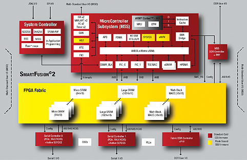
This allows the hardware-based parts of the system to be active as soon as power is restored, rather than having to wait for the FPGA configuration from external ROM.
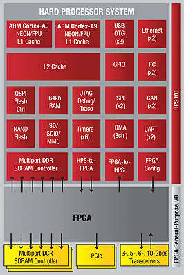
The higher-performance Cortex-A9 forms the heart of two major families of FPGAs launched recently by Altera and Xilinx. In both the Altera Cyclone SoC and Xilinx Zynq devices there are two ARM processors, allowing the devices to be used as high-performance compute engines.
As well as bringing the Cortex-M3 to the FPGA market, Microsemi was instrumental in introducing an ARM M-series MCU version for use in standard programmable logic. Optimised for implementation within an FPGA’s programmable fabric, the Cortex-M1 is a streamlined version of the Cortex-M3. The Cortex M1 is designed to not require much more die space than an 8051 core, despite being based on a 32-bit pipeline rather than 8-bit. Like the M3, the M1 runs the Thumb2 instruction set, but with some instructions and features removed. The M1 interrupt structure was simplified to save space; it supports 32 interrupt sources versus the M3’s 256.
The availability of open-source development tools has helped bring other architecture cores into FPGAs. Altera, Lattice and Xilinx each have their own RISC-like processor architectures. Each has been optimised for use within the programmable logic fabric. By bringing their compilation and linking tools into free environments such as Eclipse, the FPGA vendors make it easier for developers to switch from a standard architecture to their own.
Licensing considerations may influence which core and FPGA a designer may wish to use when the design goal is to go to a standard cell ASIC. Some soft MCUs are only licensed for use with a given FPGA supplier’s devices. This limits the ability of the designer to migrate a design to an ASIC. The advantage of these MCU cores is that they have a fully supported design and implementation flow; this makes inserting IP and subsequent development remarkably easy.
The LatticeMico32 has a more flexible licensing arrangement, which has helped to foster the architecture’s use with advocates of open-source hardware. Lattice allows the processor to be used in designs that may be migrated to ASICs supplied through independent foundries or even other FPGA architectures.
Designers need not be limited to vendor-supplied soft-processor cores. Based on the Sparc architecture originally developed by Sun Microsystems, now part of Oracle, the Leon family of cores and the OpenRISC 1200 are open-source IP blocks from independent sources. The cores typically take up more die space than LatticeMico32, Microblaze or Nios – typically 1.5 to 2 times larger in terms of logic elements used in an architecture that uses conventional four-input lookup tables – but provide flexible alternatives to the vendor-supplied cores.
As well as off-the-shelf cores, the programmable nature of the FPGA provides the designer with an excellent opportunity to build custom processors. The Cyclone SoC and Zynq architectures were developed specifically with this use in mind – devices in both families have wide I/O buses to transfer bulk data between the programmable-logic sections and the processor.
Over the years, FPGA suppliers have added support for high-speed computation, particularly for signal-processing applications.
Multipliers can consume a lot of area in a standard architecture based on lookup-table elements. The most efficient way to implement multiplication in programmable cells is to use bit-serial arithmetic. The multipliers are slow because they work by adding and shifting one bit at a time. Bit-serial multipliers excel when used in massively parallel arrays, they can support high aggregate data-rates.
The simplicity and compact nature of the bit-serial multiplier makes it possible to use many of them in a single FPGA. If latency is not important, they still make a good choice.
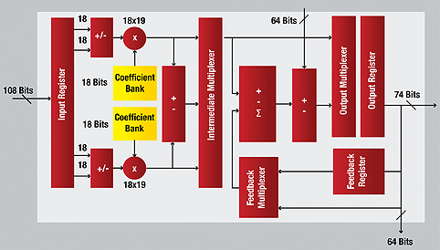
To speed up processing, FPGA vendors added carry-chain logic to let designers implement faster carry-lookahead and carry-save adders in programmable logic. Many FPGA architectures, including cost-optimised products such as the Altera Cyclone and Xilinx Spartan-6, now include hardware multiplier blocks for use in high-speed DSP applications.
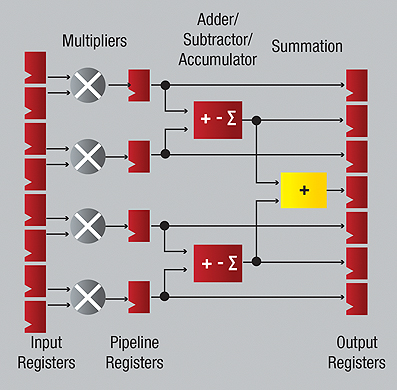
These blocks can be quite narrow to reduce their die consumption but they can easily be tied together to form more sophisticated 32-bit and 64-bit multipliers, using programmable logic cells to add support for more sophisticated features such as floating-point arithmetic. Some architectures provide a variety of DSP cores to suit target applications. These cores contain multiple narrower 9-bit units favoured for image and video processing and wider cores used for audio and communications signals.
Thanks to the programmable nature of the FPGA fabric, it is possible to build coprocessors that adapt to the needs of the system. Partial reconfiguration can allow different coprocessor blocks to be loaded into the fabric, executed and then replaced with another algorithm. For example, in an audio processing algorithm, the FPGA fabric may perform spectral processing using fast Fourier transforms (FFT) followed by filtering using a finite impulse response (FIR) filter loaded into the same section once the spectral analysis has completed.
The programmability of the fabric also helps to streamline data flow through a coprocessor element. In the case of an FFT, implementations of the algorithm in a general-purpose processor are often relatively slow because the ‘butterfly’ data-access pattern the algorithm requires involve repeated fetching and writing of temporary values in cache or main memory – the latency of those accesses may mean the internal arithmetic-logic units are starved of data. The FPGA fabric makes it possible to insert those temporary values into a complex pipeline structure that ensures DSP elements are fed with relevant data at all times.
The FPGA fabric provides advantages for operations that do not fit easily into standard ALUs. For example, cryptographic functions and many algorithms used in digital communications, such as Viterbi and Turbo decoders, often make use of modulo and other non-standard arithmetic.
With full control over the logic elements, an FGPA-based custom ALU will almost always outperform a software emulation running on a standard processor core.
The arrival of languages such as OpenCL is likely to ease the construction of coprocessor elements that can be laid out and torn up as required. Although OpenCL was developed originally to make the compute power of graphics processing units (GPUs) available to programmers more accustomed to working with general-purpose architectures such as ARM or the x86, companies such as Altera have embraced OpenCL as a way of making it easier to build custom compute engines.
OpenCL functions take the form of compute kernels – tight vector-fashioned loops that can be used to process multiple data elements in parallel. OpenCL comprises a runtime environment that loads kernels and respective data into target processors, starting execution and then fetching results once completed. Compilation tools take care of converting the algorithm expressed in the OpenCL language into an implementation suitable for configuration within an FPGA.
Another way to offload software overhead from the processor inside an FPGA is to reduce the frequency of interrupts. Each interrupt demands the processor stop whatever it is doing in order to capture or send a fragment of data through an I/O port, each interrupt involves pushing and register contents onto the stack occupying processor cycles. The analogue compute engine (ACE) in Microsemi’s SmartFusion is a small independent parallel processor that controls the various analogue I/O ports supported by the device.
The ACE combines a sample sequencing engine (SSE) with a post-processing engine (PPE). The SSE captures data from the analogue inputs, passing it to the PPE which can perform functions such as low-pass filtering, to remove noise, and transform the data into a format convenient for the processor. Devolving these functions into hardware ensures they can be used to greatly reduce the interrupt burden on the processor.
Similar techniques can, naturally, be implemented in FPGAs that lack these features to reduce the interrupt load for other processor cores. With an FPGA, there are always many ways to bring software processing and parallelised hardware speed together.
Digi-Key Corporation
www.digikey.com