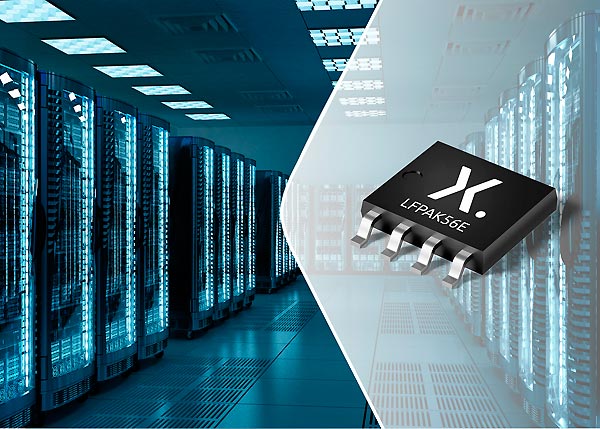
 Nexperia, the expert in essential semiconductors, today announced new 80 V and 100 V ASFETs with enhanced SOA performance, targeting hot-swap & soft-start applications in 5G telecom systems & 48 V server environments and industrial equipment needing e-fuse and battery protection.
ASFETs are a new breed of MOSFET optimized for use in particular design scenarios. By focusing on specific parameters critical to an application, sometimes at the expense of others that are less important in the same design, new levels of performance can be achieved. The new hot-swap ASFETs use a combination of Nexperia’s latest silicon technology and copper-clip package construction to significantly strengthen the Safe Operating Area (SOA) and minimize PCB area.
Previously, MOSFETs have suffered from the Spirito effect, whereby the SOA performance drops off rapidly due to thermal instability at higher voltages. Nexperia’s rugged, enhanced SOA technology eliminates the ‘Spirito-knee’, increasing SOA by 166 % at 50 V when compared to previous generations in D2PAK.
Another important advancement is the inclusion of 125 °C SOA characteristics on the datasheet. Comments Mike Becker, Senior International Product Marketing Manager at Nexperia: “SOA is traditionally only specified at 25 °C, meaning designers have to derate for operation in hot environments. Our new hot-swap ASFETs include a 125 °C SOA specification, eliminating this time-consuming task and confirming Nexperia’s excellent performance even at elevated temperatures”.
The new PSMN4R2-80YSE (80 V, 4.2 mΩ) and PSMN4R8-100YSE (100 V, 4.8 mΩ) hot-swap ASFETs are packaged in the Power-SO8 compatible LFPAK56E. The unique internal copper-clip construction of the package improves thermal and electrical performance whilst substantially reducing footprint size. The new LFPAK56E products are just 5 mm × 6 mm × 1.1 mm, offering reductions of 80 % and 75 % for PCB footprint and device height respectively, compared to the D2PAK of previous generations. The devices also feature a maximum junction temperature of 175 °C, meeting IPC9592 regulations for telecoms and industrial applications.
Adds Becker: “A further benefit is improved current sharing in high power applications that demand multiple hot-swap MOSFETs to be used in parallel, improving reliability and reducing system cost. Nexperia is widely recognized as the market leader for hot-swap MOSFETs. With these latest ASFETs, we have again raised the bar.”
The new hot-swap ASFETs are the latest devices to be fabricated on Nexperia’s new 8-inch wafer production plant in Manchester, UK, with capacity ready for volume orders. For more information, including product specs and datasheets, please visit https://www.nexperia.com/products/mosfets/application-specific-mosfets/asfets-for-hotswap-and-soft-start
You can also view this new technology in action at Nexperia’s Power Live Event 21 – 23 September https://www.nexperia.com/power-live


