


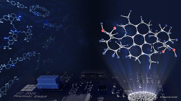
The rapid global growth rates in electronics production, combined with constantly rising quality standards and high requirements on process reliability, require new, innovative measurement methods in order to achieve a market-leading position, to stay competitive and to guarantee the highest quality standards to customers. Established testing methods, such as optical and electrical tests, often fail to detect serious quality deviations such as a high moisture content in the PCB substrate, thermal damage, insufficient degree of crosslinking or chemical impurities. However, these can be detected precisely and reliably by molecular fingerprinting with an infrared spectroscopic analysis, the so-called FT-IR analysis. An infrared spectroscopic analysis uses the principle of light absorption in the infrared range of the electromagnetic spectrum. In this process, the electromagnetic energy is converted into oscillation energy. This energy is unique for each sample as this specific molecular fingerprint. Thus, allows the clear identification of the material.
 Early detection of quality deviations with FT-IR analyses
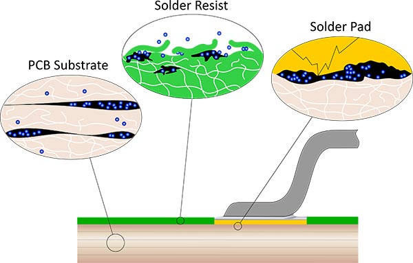 The causes of quality problems often can be found in the smallest production deviations which can easily be overlooked. Insufficient cross-linking of the PCB substrate, for example, only becomes noticeable as PCB warpage after soldering. However, the consequences are serious for the quality and lifetime of the complete board. As a result, internal stresses can lead to delamination, insufficient adhesion of solder pads and finally to an early board failure. These quality problems are also noticeable in the increased formation of condensate in the soldering machine, because non-crosslinked low-molecular compounds outgas from the PCB and polymerize, crosslink and condense in the soldering process.
In the case of solder resist, insufficient crosslinking may result, for example, in diffusion effects, an inconsistent surface and loss of the protective effect. The deviating quality is neither visually nor electrically noticeable before the soldering process. Often, an insufficiently crosslinked solder resist layer can be only noticed after cleaning process, when it does not chemically resist to the cleaning medium. Here, too, increased condensate formation of the soldering machine is an indicator of increased outgassing of non-crosslinked low-molecular compounds. The condensate layer can appear as a polymerized and crosslinked layer, as well as in the form of crystalline structures.
 Insufficient crosslinking in solder resist can have several causes. Too short a curing time is one of these causes. This results in a higher production throughput, but leads to serious quality problems in the following soldering process. Other causes are increased humidity and the influence of oxygen in the manufacturing process. Both can lead to inhibition of polymerization and crosslinking reactions. In this case, only a weakened polymerization and crosslinking reaction can be started by subsequent UV curing. Here, FT-IR analyses allow identification of the quality deviation at the molecular level and thus make an early process adjustment possible.
In practice, the quality of the finished assembly depends on numerous factors. Strict compliance of defined production requirements in PCB manufacturing is just as much a part of this as the subsequent printing, soldering and cleaning process. The combination of the PCB substrate, solder resist and solder paste is a key factor in the polymerization and crosslinking reactions of the condensate layer in the soldering system. In this way, the subsequent cleaning process of both the assemblies and the soldering system can be optimized and the cleaning medium can be used in a more resource-efficient way. Effects such as residues on the metallic surfaces of the PCB can also be avoided. This means that they can no longer lead to reduced wettability and solder bead formation in the soldering process.
FT-IR analyses – fast and cost-efficient
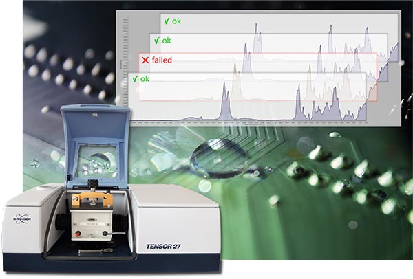
FT-IR material analyses help to detect quality deviations such as an insufficient degree of crosslinking or a high degree of humidity in the PCB substrate in time and to prevent them effectively. If a so-called “golden measurement” of the target quality is available, reference measurements of subsequent batches can be performed quickly and cost-efficiently. For the infrared spectroscopic analyses, even small sample quantities are sufficient. Precise results are available to the customer within a very short time and guarantee compliance with the highest quality standards at the molecular level.
Experience makes the key difference
Rawinski GmbH is your competent, reliable and independent partner. Our specialists will gladly support you from performing the necessary evaluations, choosing the right suppliers to analyzing the condensate residues in the soldering systems in order to extend maintenance cycles and effectively minimize cleaning costs. With many years of experience in the fields of electronics manufacturing, thermal processes, infrared spectroscopic analyses and material characterization, we are able to understand your challenges quickly and provide you with optimal support.
The result is the assurance of excellent quality in electronics production at the molecular level in order to ensure permanent market leading positions and to distinguish from market competitors in the long term.