


Connecting a development tool, laptop, and other resources to electronic hardware for test and debug is risky. While direct connections over UART, SPI, I2C, and other buses are necessary to monitor how the system behaves, there are many times when the hardware under development can fail. It can then send unwanted voltage and current over those interfaces and damage those tools and laptops.
These tools are often expensive. Not only that, but Murphy’s Law dictates that the hardware and tools will fail at the worst possible moment. The result will be a delayed project and extra expenses in overnight shipping to get the workbench back up and running.
This article will discuss how developers can protect their tool investment using interfaces based on inexpensive isolation ICs that can be built in less than 30 minutes. It will also discuss how those isolators can be selected and provide several tips and tricks to ensure that when hardware does go bad, development tools and laptops don’t go with it.
Considerations for selecting an isolator
An isolator divides a circuit into two circuits, separated by an isolation barrier. The circuits on each side of the barrier are separately powered and grounded. The barrier acts as a filter that blocks high voltages and transients, only allowing digital information or data to be transmitted from one side to the other through a coupling mechanism. The coupling mechanism is usually capacitive, magnetic, or optical.
In many cases, the reader will find that for any interface they may be interested in protecting, they will have more than a single option available to them. For example, I2C isolators are often offered in both capacitive and magnetic variants. Before selecting which technology, we need to understand the environment in which we are working.
Capacitive coupling uses a changing electric field to transmit data across the isolation barrier, which makes it a great choice in applications where there may be intense magnetic fields. Capacitive coupling also tends to result in a smaller board footprint and more energy efficient operation, both of which make it a good choice for many applications. It’s important to note, however, that capacitive coupling does sometimes have issues with noise due to a shared signal path.
Magnetic coupling uses changing magnetic fields to transmit data across the isolation barrier, which makes it a great choice in applications where there may be intense electric fields. Magnetic coupling often uses small transformers, which helps with noise rejection and a highly efficient energy transfer across the barrier.
Optical coupling uses optical pulses to transmit light across a non-conductive barrier, which makes it the perfect choice for noisy electric and magnetic environments. Unlike with magnetic and capacitively coupled signals, optical coupling can transmit steady state signals across the barrier. The disadvantages to using optical couplers are that they can be speed limited and require more power to operate.
With these different technologies and their characteristics in mind, the next step is to examine several different bus protocols and walk through how to isolate development tools on the various interfaces.
Selecting an I2C isolator
A great way for developers to develop drivers for devices outside the microcontroller is to use a bus spy tool of some sort. These tools allow a developer to monitor bus traffic. A high quality, more expensive tool will also allow a developer to inject messages onto the bus as well.
Short anecdote: I once had an I2C/SPI combo tool that was connected to a customer’s I2C bus. Their hardware failed and dropped 42 volts across the I2C bus, destroying their hardware and taking my development tool with it. Had I used an I2C isolator to protect my tools, I would not have had to spend the extra money on a new tool, and also pay for expedited shipping.
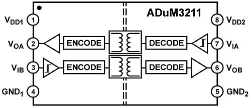
Figure 1: The ADUM3211 is a general purpose two-channel magnetic coupled isolator that can operate up to 1000 kbps. (Image source: Analog Devices)
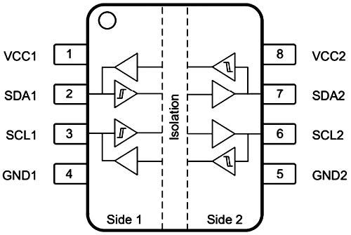
Figure 2: The ISO1541DR I2C isolator from Texas Instruments contains two bi-directional isolation channels that can operate at up to 1000 kbps. (Image source: Texas Instruments)
There are several characteristics that should be looked at when selecting an I2C isolator. First, the voltage isolation should at least be 2500 volts rms. This level of isolation will protect against 90% or more of embedded development mishaps. Second, the data rate of the isolator should be examined. Standard I2C operates at 100 kilobits per second (kbps) and 400 kbps. High-speed I2C operates at 1000 kbps. The tool or the application will determine which isolator and isolator technology is best selected.
There are several different general purpose I2C isolators that work well for protecting development tools. For a general purpose isolator, the ADUM3211ARZ-RL7 from Analog Devices is a good option (Figure 1).
The ADUM3211 uses magnetic coupling to transfer data across the barrier at data rates as high as 1000 kbps. This isolator can therefore handle high-speed I2C, but it does not contain a bi-directional barrier. This means the development tool can monitor the bus, but it cannot write to it which is perfectly fine for most applications.
To protect development tools that need to both monitor and inject data on the bus, the ISO1541DR I2C isolator from Texas Instruments is an excellent choice (Figure 2). The ISO1541 uses capacitive coupling in a SOIC-8 package to transmit bi-directional data at up to 1000 kbps. The isolator contains two separate isolation channels: one for the data signal (SDA) and one for the clock signal (SCL).
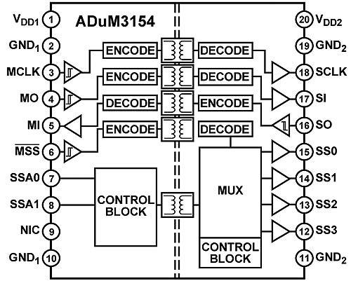
Figure 3: The ADUM3154 is a four-channel SPI isolator from Analog Devices that can handle data rates up to 17 Mbps. (Image source: Analog Devices)
Notice from both Figure 1 and Figure 2 that these devices require that the tool side provide power to its side of the isolator and that the target side power its side. Forgetting to power these from each respective source is a common reason for lack of communication across the barrier, so care should be taken during setup to ensure both sides are powered.
Selecting an SPI Isolator
The SPI bus can be a little bit trickier to protect than the I2C bus. The I2C bus contains just two communications lines, no matter how many devices are connected on the bus. The SPI bus on the other hand contains three data lines for master out, master in, and clock. In addition to these three, every device that is connected to the SPI bus requires a slave select line. It’s imperative that any SPI isolator also contain several isolation lines for the slave select lines.
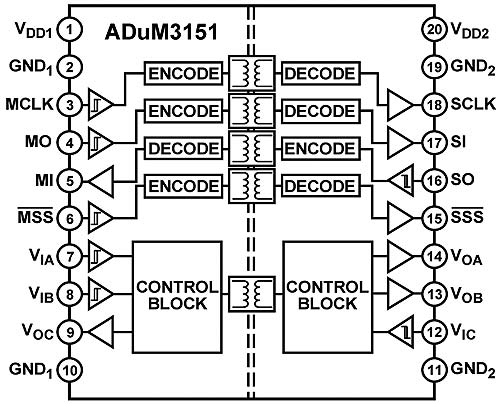
Figure 4: The ADUM3151 is a seven-channel SPI isolator from Analog Devices that can handle data rates of up to 34 Mbps. (Image source: Analog Devices)
There are several different options that fit well to protect a SPI development tool. The first is the ADUM3154 SPI isolator from Analog Devices. The ADUM3154 uses magnetic coupling to transmit data across the isolation barrier at data rates up to 17 megabits per second (Mbps). This not only covers the maximum baud rate for most microcontroller SPI peripherals of 4 Mbps, but also data rates that are common for memory interface controllers as well. The ADUM3154 also supports up to four isolated slave selects (Figure 3).
In cases where 17 Mbps is not fast enough, Analog Devices also offers the ADUM3151BRSZ-RL7 (Figure 4).
The ADUM3151 also uses magnetic coupling but can handle data rates up to 34 Mbps. It also has four channels that can be used for slave selects.
Selecting a Serial Wire Debug (SWD) isolator
One of the most expensive development tools that an embedded software engineer will usually have is a debug probe. A good debug probe can cost upwards of several thousand dollars. While the chances that something will go wrong on the programming lines is low, it’s not worth the gamble.
A developer could go and develop their own isolation solution to protect all the SWD lines, but that would be a bit time consuming and expensive. Instead, a simple solution is to use the J-Link SWD Isolator from SEGGER Microcontroller Systems (Figure 5).
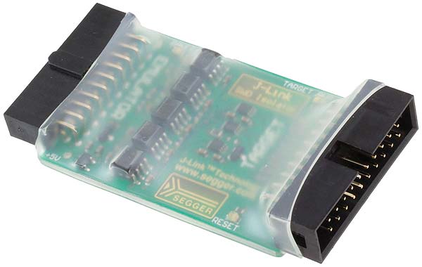
Figure 5: The SEGGER Microcontroller Systems J-Link SWD isolator provides 1000 volts of isolation between a debug programmer and the target system. (Image source: SEGGER Microcontroller Systems)
The J-Link SWD provides 1000 VDC isolation between the emulator and the target hardware.
Selecting and building a UART isolator
Many developers might consider isolating a little UART to be a waste of time and money. After all, a low-cost tool like the BOB-12731 USB-to-serial breakout board from SparkFun Electronics could easily be replaced if something happened to it. However, if something did go wrong, there could be several thousand dollars’ worth of computer equipment on the other side that should be protected. The extra time and money can be well worth it.
Putting together a UART protection circuit is simple, and similar steps can be followed to protect other bus interfaces as well. First, an isolator needs to be selected. The ADUM3211 discussed earlier is a great option because it has two high-speed isolation channels that are in opposite directions. This is perfectly suited for a UART’s Tx/Rx lines, which are often right next to each other.
Once the isolator is selected, a developer can get a breakout board like the LCQT-SOIC8-8 from Aries Electronics (Figure 6). It already includes headers and can easily be soldered onto the BOB-12731.
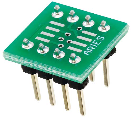
Figure 6: The Aries Electronics LCQT-SOIC8-8 provides a breakout for a SOIC-8 chip that already has jumpers on board to make a quick connection with a device target. (Image source: Aries Electronics)
When soldering the isolator onto the board and then to the UART adapter, it’s important to make sure that the voltage and ground pins align properly. If they don’t, then the isolator will not be powered. It’s also important to ensure that the isolator channel direction is in the right direction. If the breakout board or the isolator do not align properly, it may be necessary to customize a board (Figure 7).
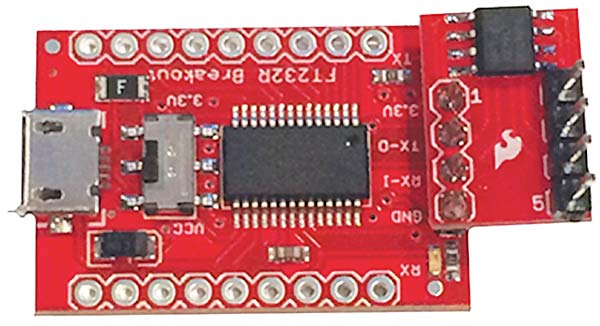
Figure 7: An assembled UART isolator circuit that has been connected to the USB to UART converter, providing customized isolated communication with the target device. (Image source: Beningo Embedded Group)
Once assembled, the USB to UART converter supplies power to the tool side of the isolator, while the target device would supply power to the target side. The result is an isolated bi-directional UART tool that is protected for up to 2500 volts.
Tips and tricks for development tool isolation
There are many techniques and isolation interfaces that can be used to protect development tools. Here are several tips and tricks to protect those investments:
- Review the datasheet and make sure that the voltage isolation specification meets your needs.
- Become familiar with the different isolation mechanisms and make sure to select the right technology for the application.
- Isolate any bus or interface that connects back to the USB port on a laptop as it is a potentially damaging ground path.
- Leverage existing development kits for the selected isolator or use breakout boards to simplify development time and cost.
- Protect a professional debugger by using an SWD isolator.
Conclusion
Many embedded systems developers don’t give a second thought to connecting an expensive development tool to a piece of hardware that is under test. Normally there won’t be any problems. However, a time will come when something unexpected happens and the development tools will be exposed to voltages and currents that exceed their specifications, resulting in damage. In order to avoid a last minute dash to get a workbench up and running, spending a few hours properly isolating tools using the many isolation solutions now available leads to a more efficient and less costly development process.
 Author: Rich Miron – Applications Engineer – Digi-Key Electronics
Rich has been in the Technical Content group since 2007 with primary responsibility for writing and editing articles, blogs and Product Training Modules. Prior to Digi-Key, he tested and qualified instrumentation and control systems for nuclear submarines. Rich holds a degree in electrical and electronics engineering from North Dakota State University in Fargo, ND.