


 Security as a high-level requirement is becoming increasingly important for more and more embedded systems as these evolve from standalone applications into connected systems capable of storing, receiving and transmitting data, updating themselves with the latest software versions, get remotely monitored and so on. Such requirements are quickly propagating even into the tiniest implementations in spite of limited memory resources and computational power.
For modern embedded developers this might be a new field, perceived as too complex to handle, whereas the very first thought while thinking of security might remind of cryptography-related topics. But in fact security-related aspects encompass many different parts of the software and chip architecture which must be designed specifically, and work together seamlessly, to achieve their goals. This article goes over the most relevant aspect to consider in relation to microcontroller security implementation in such small embedded systems.
One of the first step to secure access to a valuable asset, is to make it available under a specified usage policy. Such a policy could for example restrict which part of the application software can use it, forcing it though a defined functional interface which cannot be bypassed, and at best implemented in hardware.
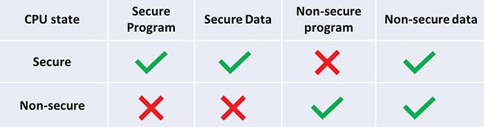
Figure 1 TrustZone access policy (© Renesas)
An example of such isolation capability is provided by Arm TrustZone technology, which allows separating the user application into a so-called “secure” and “non-secure” environment, by defining such additional state within the CPU context. Essentially the MCU memory space inherits such “security” attribute which in turn defines the access policy to a certain memory mapped address, for both code execution and data read/write. But where is the policy enforcement executed?
The match between the current processor security state and the access policy for a certain address is evaluated by a dedicated security “stage”, located within the CPU core boundary. This evaluation is done before the MCU address is transaction is propagated to the internal bus system (more to this later). If the access policy is violated, an exception (i.e. an interrupt notification) is thrown, according to Figure 1 below:
Consequently the application can react to it and depending on the requirement perform user defined actions (like re-starting a specific service, logging the event, signaling some fault to other equipment, and so on).
Looking at Figure 1, it’s easy to see that software executed in “secure” mode, has unrestricted access to data, but can directly fetch and execute instructions only from program areas defined as secure. Non-secure software can instead access only non-secure data, and execute only non-secure software. It cannot access any secure resource.
But then, how do the two words communicate with each other? The case that each environment is completely independent and autonomous from the other, seems not really meanigful; it can be expected that the non-secure application software needs to access resources and ‘services’ that are located within the secure domain. The final goal shall be to have a controlled, user defined way to let the secure and non-secure application interact with each other.
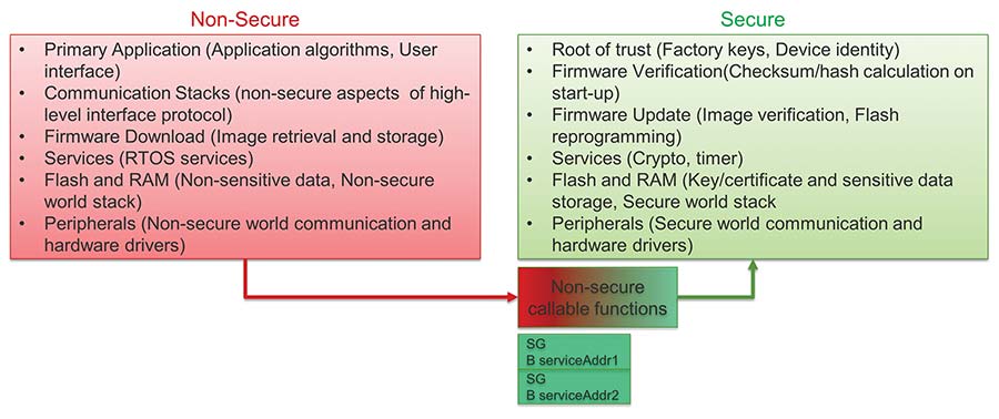
Figure 2 Non-secure callable functions (© Renesas)
Fortunately, there is a mechanism to do that. To execute any secure function, the CPU needs to change its security attribute to secure, and to do that, it uses a dedicated special instruction called ‘secure gateway’ (SG). A SG instruction is paired with an immediately following branch (i.e. ‘jump’) instruction to the desired secure function address; the non-secure application can use this ‘trampoline’ to first switch its state to secure (by executing the SG) and then to jump to the desired function, without issuing an exception. When the secure function returns, the processor state is switched back to non-secure mode.
An example of resource allocation between secure and non-secure environment is provided in Figure 2:
All pairs of ‘SG + Branch address’ instructions need to be allocated into a special area defined as non-secure callable. A non-secure callable area is secure and has such special attribute.
For the sake of details, all function parameters like memory pointers and buffer references passed by the non-secure callable functions can be tested for their security attribute, to make sure the calling function has really the proper access permissions (for example, to check that a memory buffer is really located in non-secure memory, and does not overlap over secure memory, so there is no risk of data leakage).This check can be done via a specialized ‘test target’ instruction.
Finally, it is also possible that while the CPU is in secure mode, a non-secure function needs to be called back. This would be a typical use case to notify the caller function about the status of the request, issue some RTOS-related notifications, and so on. The compiler toolchain can handle it and generate an appropriate special branch instruction that switches the state to non-secure before the call, and pushes the return address to the secure stack.
Embedded systems are heavily interrupt driven, and in such scenario we need to think of what happens when an interrupt is issued when the CPU is in a particular state. In case a non-secure interrupt happens while the CPU is in secure mode, the registers are stacked by default on the secure stack and its contents are cleared out automatically. This is to prevent unintended leakage of information from the secure area. Partitioning the exceptions (peripheral interrupts) to be assigned to the secure or non-secure environment is supported via a dedicated and separate interrupt vector table within each domain. Similarly, there is a separate implementation of the stack pointers, systick timers, and so on.
This all sounds great, but how are those secure memory areas and boundaries defined? There are two units that get interrogated in parallel: the SAU (security attribution unit) and the IDAU (implementation-defined attribution unit). On each CPU access, both units perform an address lookup and respond with the security attribute associated with that address. The response of the two units gets combined, to define the address attribute; the overall principle is that the stricter of the two wins (meaning it is not possible to ‘override’ a secure region setting with a less secure attribute). Finally, the combined security attribute for that address is evaluated against the policy defined as in figure 1. If the access is legitimate, it can proceed – otherwise, it is blocked and an exception (secure interrupt) is raised at the CPU level.
Noticeably, the configuration of the SAU (how many regions are supported, the default settings, etc) can be defined at design time, and the implementation of the IDAU is implementaiton defined, i.e. left to the device manufacturer.
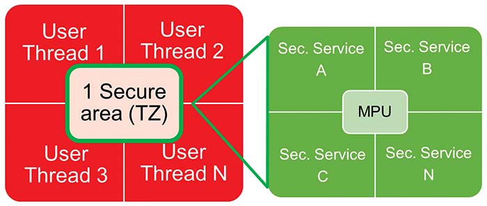
Figure 3 TrustZone and MPU partitioning (© Renesas)
For further partitioning of application tasks, memory protection units (MPUs) can be used within each domain, to protect individual threads from each other, and enhance the overall robustness of the software against errors. Figure 3 shows how the software application could be partitioned on a microcontroller supporting TrustZone:
Have we achieved any security related goal so far? Actually, not yet. TrustZone provides isolation between application threads executing in the secure environment, and those executing into the non-secure environment. But it does not provide any “security” per-se and cannot control which threads access the secure environment, i.e. it cannot enforce legitimacy; rather prevent unintended usage or direct access to resources.
At the end, it is the developer’s decision, which part of the application shall be isolated, and this is highly application dependent. TZ isolation can be used to protect any assets and enhance the reliability of an application, compared to a classical MPU based approach which relies on a priviledge level only (but is fairly easy to modify and circumvent in software). On the other hand, putting inside TrustZone area the cryptographic related operation seems a good idea for most applications requring crypto. Important is that the system shall apply any such settings right from the start of execution (at reset), and the configuration of such boundaries cannot be tampered with. Those could for example get stored into a special memory area not directly modifiable by the CPU itself.
For typical security (cryptographical) related requirements, good practice would suggest keeping the amount of functionality implemented within the secure environment as essential and minimal as possible. This to reduce the possibility of misbehavior due to bugs in software implementation, runtime errors, and the malicious exploiting of any software defects by an attacker trying to gain unauthorized access to MCU resources. As a side effect, following this principle also makes validation of the functionality much easier during debug and test, since there is less to test.
Which resources shall a cryptography capable microcontroller provide? It depends on the application complexity, as for an entry level solution, a pure software routine might be used as well. But having support for cryptographic algorithms in hardware has many advantages in terms of power consumption, code size and responsiveness of the system thanks to higher execution speed.
Having said that, the first building block of most cryptographic protocols is a TRNG (true random number generator), which shall be validated and tested for its entropy properties and quality of randomness (since an ill-constructed RNG can spoil the security of any algorithm using it).
For local storage, support of symmetric algorithms like AES with multiple operation modes is almost mandatory, to encrypt and decrypt bulk of data. In combination with hashing algorithms (a sort of cryptographically secure checksums) like SHA-2 or SHA-3 can be perform simple authentication checks and verify that the contents of data have not been modified.
For more advanced connectivity, the device shall support asymmetric encryption algorithms like RSA or ECC (elliptic curve cryptography) to support identity verification in client / server connections, derive secrets to generate ephemeral session keys, or verify the source and legitimacy of a firmware update, for example. All those accelerators shall also be able to generate user keys on-chip, for local usage.
In any case, the hard problem behind their use is the key management. The most valuable asset represented by the user key must be protected by keeping its confidentiality (not exposing its value), its integrity (not allowing the key to be unnoticeably modified) and ensuring its availability. This opens lots of scenarios to consider, from when the key is injected (stored) in the system, how it gets transported there, how it gets loaded in the cryptographic hardware and protected from leakage during operation.
Ideally the key material shall not be handled by the application software in plain text, i.e. in clear format, since it will be dangerously exposed. A simple way to prevent this could be to handle the key within the secure area defined by TrustZone, but best would be use the keys only within a dedicated subsystem isolated from the rest. A similar problem raises once the keys are (typically) stored in the non-volatile memory; to avoid a break of confidentiality, techniques like key “wrapping” (essentially, key encryption) can help to protect the user key privacy. Making the wrapped data unique on every MCU further helps against shared keys leakage, and eliminates the risk of key copying (cloning) from an existing system to another. Obviously to implement such mechanism a ‘root of trust’ for storage is mandatory, therefore the cryptographic subsystem must have exclusive access to a ‘key encryption key’ unique for each microcontroller. The root of trust being unique per each MCU avoids that a compromise in one specific device allows a ‘class’ attack on all equipments fitting the same unit.
Another important aspect is to assess the robustness of the crypto subsystem against DPA and SPA attacks, which log and analyze the power consumption traces and can reverse-engineer the key value. This type of attacks are getting increasingly cheap and quick to implement, even for non-highly skilled attackers with limited resources. If physical access to the device is of concern, and there are no other access control means in the system, countermeasures against those those threats should be available and used. Additionally, any early detection feature which can monitor IOs connected to the equipment housing, generate a notification to the system, and possibly take a timestamp when a tamper is detected, will be desirable as well.
To make the user life easier, the subsystem shall allow a way to provision, i.e. ‘inject’ user chosen keys into the device and have those wrapped and securely stored, ready for later application usage. The microcontroller should support some interface to provision the keys both in field and in factory, allowing easy first-time production, and later provisioing and updating in the field. Such provisioning step shall be secured as well, i.e. not expose any key content while this is in transit to the MCU.
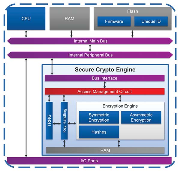
Figure 4 Secure Crypto Engine (© Renesas)
Considering now the software implementation, the mentioned approaches so far focused on the main CPU executing the application software. But in modern microcontrollers, other functional entities are able to autonomously transfer data to and from memory or peripherals, to improve performance by more efficiently using the available bandwidth. Some examples include DMA engines, graphics controllers, ethernet controllers and such. All the isolation features related to TrustZone are meaning-less for those agents, since these can issue transactions on the main interconnect bus autonomously and irrespectively of the CPU security attribution units, withouth further countermeasures. Therefore, it is vitally important that the microcontroller implements options to define the security attribute of each of those master peripheral channels, and has specific “filters” located on the slave side of the communication (in front of memories and memory mapped periperhals). Violations of the access policies at system level also need to be able to trigger exceptions (i.e. interrupt notifications) to the main CPU, in order to take corrective actions.
Any microcontroller system would be almost useless without the capability of performing input and output operations on external digital and analog signals. Protecting such interfaces from misuse is also a fundamental requirement to prevent tampering, as this is obvoiusly the pre-defined way to interact with the MCU. The wary designer should make sure that the microcontroller can restrict the access levels for the I/O ports and peripherals, to prevent software to maliciously ‘take control’ of an interface, interfere with it, or snoop the communication (thereby breaking the security policy). The implemented functionality shall allow to isolate the peripherals and their ports from each other securely. Keeping in mind space constraints, especially in small microcontroller packages the amount of functional interfaces can be much higher than the number of phisical pins available on the package; many of those are multiplexed together for the user to choose from.
During the development phase, to test the software and verify it behaves as expected, a Jtag based debug probe is almost mandatory. By its very definition, such interface is able to access almost all resources on the chip and therefore constitutes a significant backdoor for any application which is later deployed in the field. The use cases for securing Jtag might be very different: some would want to permanently lock it, others might want to keep debug capability in the field and simply protect the access. Whatever strategy is chosen, it shall not be possible to bypass a permanent protection or access it without proper authorization; an authentication code or key owned by the developer shall be required in a challenge-response mechanism, and the latter shall complete succesfully to enable any successive communication. Finally, the device shall support a secure mechanism to send the device back to the factory for further analysis, in case a product defect is suspected; this might involve erasing any stored secret assets, by still keeping the interface secured.
After development, the final application image is ready to be deployed in the field. Part of it might be subject to later updates, but part of it shall be immutable to ensure that the application or the boot loader code is in a well-known state at any time. To support this requirement, the microcontroller shall have the capability to permanently protect user-defined parts of the non-volatile memory from modification.
Last but not least, each microcontroller undergoes a lenghty test process in factory, to verify its correct functioning according to the techincal specification. At the same time, many results of such tests (like trimming values, production specific data etc) and other MCU related settings are stored on the device during such factory test. This special test mode is not meaningful to an end user, but being very powerful it can access, control, and potentially tamper all chip resources. From security perspective, this is another potential backdoor and the manufacturer should ensure that a test mode cannot be entered maliciously or by mistake, once the device is out of the factory and in customer’s hands.
Searching for the appropriate microcontroller supporting all or most of the above requirements can be a daunting task. Fortunately, Renesas has designed the RA series of microcontroller exactly with such goals. The RA6 and RA4 series of Renesas microcontrollers include devices featuring an ARM Cortex-M33 CPU with TrustZone and secure Memory Protection Units. They allow programming secure and non-secure boundaries and settings for all built-in memory types in an easy and simple way. They embed the Secure Crypto Engine, a crypto subsystem (depicted in Figure 4) which provides comparable secure element functionality at higher performance and less bill of material cost. The SCE includes state of the art cryptographic algorithm accelerators, a TRNG, key generation, key injection in factory, SPA/DPA countermeasures, and implements a secure hardware root of trust by means of a hardware unique key. At system level DMA controllers, bus masters, peripherals and I/O pins have dedicated security attributes, tamper detection functionality is implemented. The MCU implements a device lifecycle management with integrated handling of secure/non-secure debugging, secure/non-secure programming, return material procedure and protection of test mode. Any non-volatile memory block can be made permanently protected at user discretion, thereby allowing a flexible Root Of Trust definition. For more information about the RA family security features, please visit www.renesas.com/RA
Bibliography
Evaluation Kit for RA6M4 MCU Group.
R01UH0890EJ0110 RA6M4 Group User’s Manual: Hardware.
R01AN5562EJ0100 Standard Boot Firmware for the RA family MCUs Based on Arm® Cortex®-M33
Author: Giancarlo Parodi
Renesas Electronics Europe | https://www.renesas.com
![]()