


 Alphawave Semi, a global leader in high-speed connectivity and compute silicon for the world’s technology infrastructure, has announced the expansion of its strategic partnership with Samsung Foundry, one of the world’s leading advanced semiconductor manufacturers.
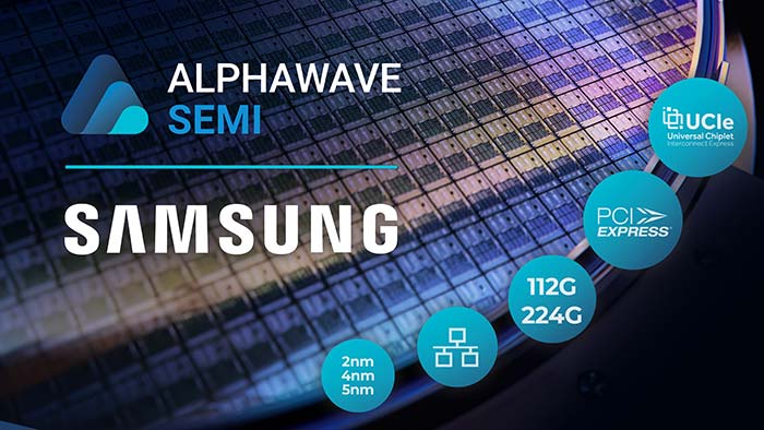
The expanded agreement encompasses leading-edge IP for PCI Express 7.0, 112G and 224G Ethernet and the latest UCIe (Universal Chiplet Interconnect Express) die-to-die interconnect standard that is enabling next-generation SoC (system-on-chip) technologies for AI and other HPC systems.
Alphawave Semi’s partnership with Samsung Foundry is based on an extensive range of IP aimed at minimizing design risks and propelling the success of high-performance silicon and next-generation chiplets for sectors such as artificial intelligence (AI), high-performance computing (HPC), data networking, autonomous vehicles and solid-state storage (SSD). The latest expansion of the collaboration expands these offerings for Samsung’s cutting-edge SF5 (5nm), SF4 (4nm), and SF2 (2nm) processes with additional, state-of-the-art IP that is essential for next-generation compute and network connectivity.
“Strengthening our collaboration with Samsung Foundry marks a significant step forward in our mission to drive the future of high-speed connectivity,” said Alphawave Semi CTO Tony Chan Carusone. “This partnership leverages both Alphawave Semi’s leading-edge IP portfolio and Samsung’s manufacturing prowess to meet the fast-growing demands of high-performance computing and networking.”
For more information about Alphawave Semi and our partnership with Samsung Foundry, please visit www.awavesemi.com