


I’m willing to bet that there are tens of thousands of analog applications out there that would benefit financially from ASIC integration. So what’s the holdup? Based on my 40+ years in the Analog IC business, I can boil it down to one word: misinformation. This is a combination of a lack of information, incorrect information, and of course, FUD (Fear, Uncertainty and Doubt). Misinformation comes from numerous unreliable sources. It’s high time we dispel the myths that often precede incorrect decision making and expose the bare-bones truth about Analog ASIC integration. Most of the time, it’s the sensible thing to do, but confusion about all the preparatory steps you must take leading up to getting a proposal for NRE and Tooling is often an early show stopper.
By Bob Frostholm, JVD Semiconductors
Proper planning in anticipation of having an Analog ASIC developed and produced for your company is not to be taken lightly. There are five key elements you need to explore internally before engaging an Analog ASIC semiconductor company to design and produce a custom chip for you. Once you are comfortable with this internal analysis, you can then explore possible suppliers. If you’ve done the internal analysis correctly, you will have realized that there is much more to Non-Recurring Engineering (NRE) than the upfront costs your supplier will charge you for designing and tooling a custom chip. That’s the easy part, because it’s spelled out clearly in black and white in the contract you’ll be signing at the beginning of the project. There is a hidden part of NRE that few companies successfully quantify. And for good reason – it’s not easy. Let’s take a moment and examine some of the more important aspects before going into what’s behind the ‘green curtain’: the effort put forth by your Analog ASIC supplier.
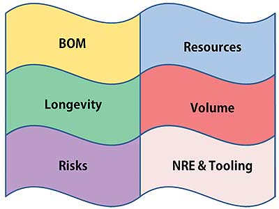
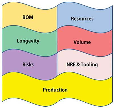
There are several pieces to the ASIC puzzle, and they must all fit together before a proper decision to move forward can be made.
Identify your existing BOM costs. When asked, most customers simply get a list of components from their purchasing department along with the price they currently pay for them. Less obvious are the ‘other’ costs associated with these components. For example: purchasing costs, inventory costs, manufacturing costs including labor costs (whether human or machine), cost per square inch of the PCB, or cost of lost production when there is an availability or quality problem from a supplier. This last one is really difficult to put a financial metric on. Consider as well the other side of the coin; there are BOM
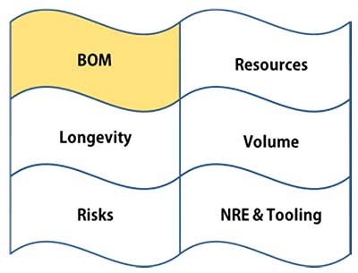
costs associated with an ASIC as well. A new PCB layout is required. Perhaps additional qualification and reliability testing will be involved. All of these costs need to be scrutinized closely by both you, and the customer when considering a move to an ASIC solution. Be sure to quantify ALL the costs you will incur as well as all the costs you will save before committing.
Identify availability of your resources to manage the transition from using many standard chips to a single ASIC. Someone needs to be the focal point when dealing with the ASIC company to field technical questions and answers, define the electrical specification for the ASIC, conduct progress reviews and design reviews, manage the production change over, and much more. Program management does not necessarily require an additional headcount, but it will become a significant responsibility assigned to someone on the team. Be sure you have someone capable to assume this role and have a backup plan in case this person
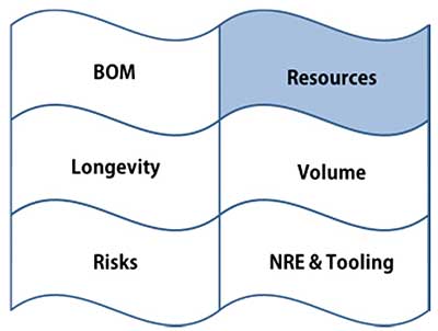
leaves in the future.
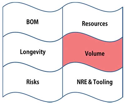
Understand the longevity and cumulative volume expectations of your product. There’s not much point incurring the effort to develop an ASIC if its lifespan will be too short. There are, of course, obvious exceptions, such as applications in which the volumes are vast, as in mobile phones and computers. There, if the lifetime of a chip is only a couple of years, the savings clearly justify the transition. I suspect most readers of this paper can only dream of such volumes. The good news is that Analog Applications typically have long lifespans and can easily support and justify the transition to an ASIC chip. Many industrial and medical applications can last 10 years or longer.
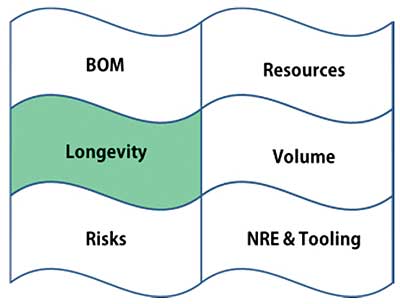
Don’t over estimate your volume expectations to try to lure an ASIC supplier into engaging with you. It is always better to underestimate; err on the conservative side. Analog ASICs do not require high volume. While everyone’s definition of “high volume” varies, to quantify it, many projects are successful at 25-50K units per year, even less occasionally. The days of million or half million or even 100K per year unit minimums are long gone. Analog ASICs have always been affordable to the masses. The problem has been that the masses never realized it. This is perhaps the single biggest misconception about Analog ASICs.
As the customer, your responsibility is to manage as best you can the above four puzzle
pieces. The fifth piece, Risk, is a shared piece. Both Customer and Supplier must do all that is within their power to mitigate risk. Analyze the risks associated with ASIC development on both sides. What if your volume expectations aren’t realized? What if your Analog ASIC supplier is unable to meet their completion date? Or worse yet (as is all too often the case) doesn’t really have the resident Analog skill sets to complete the job, meeting all your technical requirements? Asking for last minute waivers can kill your entire project. You can avoid this by investing in advanced research. Ask to speak to the leader of the ASIC design team that will be assigned to your project and assess for yourself their skills and understanding of analog chip design. Check references. Make sure they fully understand your application.
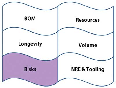
What if you need to make a design change midway through the ASIC development process? This happens frequently. Things can go wrong, and often do. Requirements can change unexpectedly. Make sure both you and your Analog ASIC supplier understand this and have a corrective action plan. There may be additional charges, depending on the changes you are requesting and how far along the design is. If the chip needs a re-spin and you didn’t change your requirements, it’s the responsibility of the ASIC supplier to do it without charging more. Remember, it’s the ASIC supplier’s responsibility to both hire and retain the best design talent as well as utilize the highest quality subcontractors for silicon fabrication and package assembly. If there are any problems there, they own it, not you.
This is where Analog differs greatly from Digital in the ASIC world. Parametric performance in the digital world is almost a no-brainer. Every function that connects to another function has a well-defined interface. It’s either a logic 1 or a logic 0 and each of these has a well-defined min and max limit. This is not the case with Analog. Analog design requires that thousands, possibly tens or hundreds of thousands, of device interconnects on the chip match exactly.
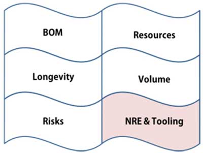
What does this mean for NRE? What it means is that when specifying and designing Analog ASICs, there is significantly more CUSTOM ENGINEERING involved. It also means that much more care and consideration must be put into the budgetary proposal being prepared for the customer. It’s not unusual for back and forth technical Q&A to take place between the lead ASIC designer assigned to the project and the customer’s point person. The ASIC supplier needs to know everything there is to know about the design: its application, its environment, its architecture, and more. This process of thoroughly understanding the customer’s needs can take weeks, sometimes months before a legitimate proposal can be offered. When quoting a moderate to complex Analog ASIC, it’s not unusual for the ASIC supplier to invest $10-$20K of their own resources just to provide a proposal. They should not be charging you for this effort, it’s part of the cost of doing business.
Moreover, while the ASIC design manager is evaluating the basic ASIC itself, another ASIC team is looking into how this chip is going to be tested. What levels of precision are needed? Are there any special needs such as data acquisition functions? What power management blocks are involved? Are there any special noise requirements? Power up sequences? Are there any high voltage requirements that need to be addressed? At the end, does a special analog tester need to be designed and built beyond a typical load board?
The cost of the NRE and Tooling can vary greatly. Variables include the design complexity (man hours required to design and layout the chip), mask costs (determined primarily by the lithography of the wafer process; 0.18um, 0.35um, 0.5um, etc.), wafer costs (determined in part by the wafer size (150mm, 200mm, etc.), and by special needs (number of layers, SOI, cavity etch for sensors, etc.). Your Analog ASIC supplier will review with you any options and tradeoffs you may wish to consider that might minimize any of these costs.
Another thing to consider is NRE and Tooling Rebates. Ask you Analog ASIC supplier if they offer a rebate program for the up-front costs associated with developing the chip. These are implemented during the early production lifetime of the product, and are a means of further equalizing the cost of an ASIC with that of a standard product. It essentially has the effect of making the front end costs appear as a loan that gets paid back as production is consumed rather than a sunk cost.
Supporting all of this is production capability. During this proposal development phase, the ASIC design manager also investigates the realm of possible wafer fabrication processes that are suitable to produce your design, selecting the one she/he feels is a
best fit solution. The IC will be designed to meet the specific requirements of this silicon process. With rare exception, silicon fab processes cannot be changed or modified.
The burden is 100% on the ASIC design team to get it right. If you remember only one thing from this paper, it is to NEVER SEPARATE DESIGN FROM PRODUCTION. Doing so sets the stage for conflict when something goes wrong. Is it a design problem or a manufacturing problem? Unless your Analog ASIC supplier is developing or modifying a process, when a performance issue arises in the initial silicon samples, 99 times out of 100 it will be a design problem. Yet independent Analog design houses will argue the contrary, and you, the customer, are stuck in the middle. This is not where you want to be. Even if you have lots of experience managing the backend for digital ASICs, you should always use full service or turn-key supplier for Analog ASICs.
Unlike digital ASICs, Analog designs are extremely difficult (dare I say impossible?) to port to a fabrication process other than the one they were originally designed for without doing a major redesign or re-layout of the chip. For this reason, selection of a reputable foundry, one with a solid track record of Analog IC production, is paramount. During the chip’s design phase, the ASIC design team also considers the longevity of the process being selected. Is it well established? Meaning has it been in production for a long time and has it been proven to be reliable? Does the foundry have considerable volume running on this process such that its likelihood of being discontinued is zero? All of the above helps you to mitigate the risks.
Once you have accepted the ASIC development and production proposal, a detailed specification of the IC is generated. This specification is similar to a typical semiconductor datasheet in terms of its contents. There may be a brief description of the IC, and a definition of the MAX operating limits (temperature, voltage, etc.) followed by a detailed electrical specification. The accuracy and completeness of the electrical specification is critical because this is what is used to define accept/reject criteria for the ASIC. The electrical specification becomes a part of the development contract, usually as one of several “Exhibits” attached at the end of the contract. It is not unusual for minor changes to be made to the electrical specification (but only by mutual agreement) during the development of the chip as one side or the other notices things that may be mutually exclusive, or as one side discovers a means by which the chip can be further improved or reduced in size.
When the electrical specification is finalized and the contract is signed, development begins. Weekly, sometimes daily, discussions between the ASIC supplier and customer keep both sides in synchronicity throughout the development period. Periodic milestone reviews are held as well as a final signoff review, at which point the design is declared finished and the hard tooling / wafer fabrication phase begins.
Once the foundry has produced the masks, they will begin wafer production. Throughput can vary from 8 to 12 weeks before a finished wafer is delivered back to the ASIC supplier for testing. If all has gone according to plan, the ASIC supplier will have the test system finished and awaiting wafers to test. Thanks to the skills of experienced Analog Design Engineers, 99% of designs are fully functional in this first look. However, with analog, almost all designs will require minor tweaks to achieve complete parametric compliance with the specification…
It’s just the nature of the beast… Although analog design and verification tools from companies like Cadence, Synopsys, Mentor Graphics, and others continue to improve, none are perfect. Still, a lot can be learned from a functional part. Samples are prepared and sent to the customer for evaluation. Any nonconformities or performance nuances are noted and normally corrected with a minor tweak to the metal layers of the chip. Upon verification by the customer, the revised chip is released to production.
Advanced planning, thoughtful and proper resource allocation, intimate understanding of your supplier’s Analog Design and production skills, a well-defined objective specification, and more will ensure the success for your project.
A couple of side notes to file away in your memory;
1. When it comes to Analog, there are no shortcuts. If you insist on beating up your chosen supplier to quote shorter and shorter development times, it may backfire on you. Although delivery of first samples sometimes occurs in as little six to eight months, realistically you should expect it to be closer to ten to twelve months and even longer for very complicated designs. Individual quotes will vary.
2. Think about your IP. If your design is simply an amalgamation of off the shelf standard products with no inherent invention in the design, you may not care. But if the chip will be containing your own proprietary IP, check very carefully as to where your chip will be designed. Yes, engineers in the US and EU may be more costly, but what are the costs to you and your business if your design is stolen? Have you ever wonder how products like the new Apple watch become available for sale on Alibaba before being released?
The same holds true for wafer fabrication. If you are at all concerned, insist that the product be fabricated where the Rules of International Law apply.
3. Don’t be pennywise and pound foolish. When having an Analog ASIC made for you, be very thorough about whom you select to design and build it. The cheapest solution may not be the best solution.
—————————————————————————————–

Bob Frostholm is Vice President of Marketing & Sales at JVD Semiconductors, (San Jose, CA.) www.jvdinc.com
Bob has held Marketing, Sales and CEO roles at established and startup Analog Semiconductor Companies for more than 40 years. Bob was one of the original marketers behind the ubiquitous 555 timer chip. After 12 years with Signetics-Phillips, Fairchild and National Semiconductor, he co-founded his first startup in 1984, Scottish based Integrated Power, which was sold to Seagate in 1987. He subsequently joined Sprague’s semiconductor operations in Massachusetts and helped spin off its semiconductor group, creating what is now known as Allegro Microsystems and later helped LSI Logic acquire SEEQ Technology. Bob has been consulting with numerous start-ups until joining JVD in 2010. He is the author of several technical articles and white papers as well as numerous short and feature length screenplays. Bob is also a member of the Engineering Advisory Board of the College of Science and Engineering, San Francisco State University.