
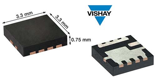
 Vishay Intertechnology, Inc. today introduced a versatile new 30 V n-channel TrenchFET® Gen V power MOSFET that delivers increased power density and enhanced thermal performance for industrial, computer, consumer, and telecom applications. Featuring source flip technology in the 3.3 mm by 3.3 mm PowerPAK® 1212-F package, the Vishay Siliconix SiSD5300DN provides best in class on-resistance of 0.71 mΩ at 10 V and on-resistance times gate charge — a critical figure of merit (FOM) for MOSFETs used in switching applications — of 42 mΩ*nC.
Occupying the same footprint as the PowerPAK 1212-8S, the device released today offers 18 % lower on-resistance to increase power density, while its source flip technology reduces thermal resistance by 63°C/W to 56°C/W. In addition, the SiSD5300DN’s FOM represents a 35 % improvement over previous-generation devices, which translates into reduced conduction and switching losses to save energy in power conversion applications.
PowerPAK 1212-F source flip technology reverses the usual proportions of the ground and source pads, extending the area of the ground pad to provide a more efficient thermal dissipation path and thus promoting cooler operation. At the same time, the PowerPAK 1212-F minimizes the extent of the switching area, which helps to reduce the impact of trace noise. In the PowerPAK 1212-F package specifically, the source pad dimension increases by a factor of 10, from 0.36 mm² to 4.13 mm², enabling a commensurate improvement in thermal performance. The PowerPAK 1212-F’s center gate design also simplifies parallelization of multiple devices on a single-layer PCB.
The source flip PowerPAK 1212-F package of the SiSD5300DN is especially suitable for applications such as secondary rectification, active clamp battery management systems (BMS), buck and BLDC converters, OR-ing FETs, motor drives, and load switches. Typical end products include welding equipment and power tools; servers, edge devices, supercomputers, and tablets; lawnmowers and cleaning robots; and radio base stations.
The device is 100% RG- and UIS-tested, RoHS-compliant, and halogen-free.
Key Specification Table:
| PowerPAK 1212-F | PowerPAK 1212-8S |
| Package size: 3.3 mm x 3.3 mm | Package size: 3.3 mm x 3.3 mm |
| Source pad dimension: 4.13 mm² | Source pad dimension: 0.36 mm² |
| Thermal resistance: 56 °C/W | Thermal resistance: 63 °C/W |
| Lowest available on-resistance in Gen V technology: SiSD5300DN: 0.87 mΩ (maximum) |
Lowest available on-resistance in Gen V technology: SiSS54DN: 1.06 mΩ (maximum) |
Samples and production quantities of the SiSD5300DN are available now, with lead times of 26 weeks.