


Texas Instruments introduce a new athlete to the embedded memory arena, called FRAM – ferroelectric random access memory, with amazing abilities. Looking at five disciplines we will compare this sportsman’s performance against his long time established Flash opponent. Before we go there let’s “x-ray” our two athletes to understand how they work.
By Matthias Poppel, Texas Instruments
How does FRAM work compared to Flash?
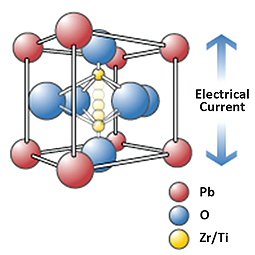
FRAM is built up similarly to DRAM consisting out of a transistor switching the current and a capacitor storing the information. Different is the capacitor’s dielectric which uses a ferroelectric material called Lead Zirconate Titanate, PZT. The term “ferroelectric” must not be confused with “ferromagnetic”. Only the relationship between voltage and charge of ferroelectric material looks similar to the hysteresis shape of ferromagnetic material. FRAM does not contain iron and is not susceptible to magnetic fields. In the presence of an electrical field a dipole inside the crystal gets formed by a shift of atoms and electronic charge along the direction of the field. The two possible polarization stages represent the logic “1” or “0”. FRAM is non-volatile as this polarization remains robustly even when the electrical field is removed. “Switching” the dipole is fast and requires only little energy.
A Flash memory cell – NOR Flash is typically used in microcontrollers – consists of a single MOSFET with two gates stacked on top of each other. The Control Gate switches the current from source to drain like in a normal NMOS transistor. The Floating Gate underneath the Control Gate is completely insulated by an oxide. Logic “1” is represented by no charge on the Floating Gate. Applying a threshold voltage to the Control Gate switches on the channel and flowing current can be measured. To program the cell to logic “0” a higher voltage, typically 12-14V, gets applied to the Control Gate. Now the source-drain current becomes high enough that some electrons jump through the oxide onto the Floating Gate.
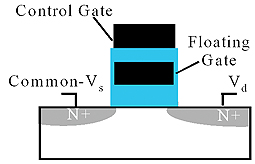
This process is called hot-electron injection. The charge on the Floating Gate will drain the channel in a normal read operation so that not enough current can be measured to detect logic “1”. Erasing the Flash back to logic “0” – usually only possible in a block of cells called sector – gets achieved by applying the high programming voltage with opposite polarity causing electrons to move off the Floating Gate by quantum tunneling. Programming and erasing Flash memory takes some time and requires higher voltages that on-chip charge pumps provide from the supply voltage. Electrons on the Floating Gate containing the binary information stay there reliably for years but any weakness in the insulating oxide or physical effect by radiation for instance causing electrons to leak on or off the Floating Gate can cause a so called “bit flip”.
The FRAM Pentathlon
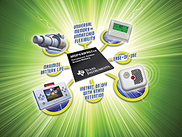
The universal athlete
Who in the embedded processing market doesn’t know the questions arising already at the beginning of a project when it comes to processor selection, and especially its memory configuration? How much non-volatile memory for program and data will we need? How big is the boot loader program? How much memory head room for additional features will we need, or shall we use external Flash and only on-chip SRAM? How much SRAM will we need at run time for the program, for data, as scratch pad? Do we have log data at high occurring frequencies that we want to constantly overwrite and do we need to allocate external EEPROM for that purpose?
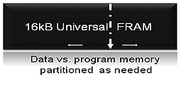
With FRAM we now have a universal player, regardless whether Flash, SRAM, or EEPROM was used before. FRAM is non-volatile, it keeps its content after power down. The MSP430FR57xx family buffers enough on-chip energy to finalize a writing operation to memory even during loss of power thus maintaining a defined state. On top, designers do not have to worry about sector sizes and sector erase limitations as FRAM even offers bit programming. Designers are free to partition the entire on-chip memory according to their needs.
Almost no food
In an experiment we are writing data at a speed of 13kB per second to the FRAM of the MSP430FR5739 in one case and to the Flash of the MSP430F2274 in the other. Below diagram shows the current consumption needed in both cases.
Assuming 9uA compare to a single banana that our FRAM athlete needs to carry along as energy reservoir, to perform the same task the Flash opponent will have to carry a large backpack of 244 bananas. What a nice weight advantage that everybody who tried running in his life would appreciate.
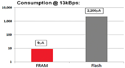
Back to the embedded processing world this means additional significant power savings as memory access is an essential function in any microcontroller application. Main reason for the ultra low power memory operation is that FRAM needs little energy and gets programmed at 1.4V while Flash requires a charge pump to supply the programming voltages of 12-14V.
The 400m sprint champion
We are again comparing our two opponents from the previous experiment. Now we are writing 64bytes of data to the FRAM and Flash respectively, measuring the time needed. Writing to the memory of the MSP430FR5738 takes 1.6usec and flashing the memory of MSP430F5438 takes about 1.6msec. Flipping the dipole in the FRAM crystal is fast compared to driving charge through a thick oxide onto a floating gate.
To picture the difference, we put our two athletes into a 400m dash contest. Both are ready, hovering over the ground, awaiting the starter’s gun. At the signal, our Flash runner is still busy with his human reaction time and hasn’t yet left the starting block while the FRAM runner has almost finished his 3rd round. By the time the Flash runner is closing in on his first 400m lap – at world record speed – the FRAM runner has just passed one thousand laps.
Low power applications will benefit from this extremely fast write time as processor wake up periods can be shortened thus extending battery life time. Another advantage is saving time and money during in-line programming, where time to download code into the device can be significantly shortened.
The marathon
From the sprint we move to the endurance discipline. Flash write/erase cycles for embedded memory is limited to 10.000 cycles, in some exceptional cases to 100.000 cycles. FRAM however has a write endurance of at least 1014 cycles.
Trying to visualize the difference between those numbers we assume 105 cycles represent the endurance it takes to run a marathon of 42km. While our Flash runner takes on the distance between Marathon and Athens, the FRAM runner circles our planet along the equator, not only once but a million times.
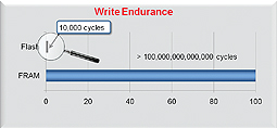
The FRAM dipole mechanism is very robust and doesn’t show any wear effect at 1014 cycles. There are even studies showing this technology going beyond 1016 cycles. This write endurance is far more what any application requires from non-volatile memory today. However, Flash is not the only memory type FRAM needs to compete with. As we want to use FRAM also like SRAM as part of the universal memory we need to look at required SRAM cycles. In battery operated equipment for instance a 10% active duty cycle accessing the same memory location at 8Mhz would lead to a life time of about 8 years at 1014 cycles and to about 80 years at 1016 cycles.
The armored player
Our FRAM athlete is not only fast, perennial, and frugal when it comes to energy consumption but also very robust and armored like a football player.

As described above FRAM does not contain iron and is not ferromagnetic. FRAM therefore is not affected by magnetic fields. Susceptibility to electrical fields is also very low. Even a 50kV field in immediate proximity is not able to introduce enough voltage to impact the memory cell. The phenomenon of alpha particles, ions, cosmic, gamma, or x-rays causing a bit cell to flip to an opposite state is called “soft error”, and the occurring rate “Soft Error Rate” – SER. Any memory technology using charge on a capacitor can get affected. Not so for FRAM. It is unlikely that a particle will hit the FRAM dipole and change its polarization. Terrestrial SER for FRAM is not even measurable.
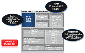
TI’s MSP430 ultra low power microcontroller goes FRAM
Embedded processing is not an individual sport. Every star player needs a team. Inserting FRAM into MSP430 microcontrollers augments this family’s low power, high performance DNA perfectly. The first MSP430FR57xx FRAM product line that is available now features the well known 16bit MSP430 core running at 24MHz consuming only 100uA/MHz. The fast FRAM write speeds at low power help even further reduce time periods the processor needs to stay awake thus extending battery life time or even enabling new applications like energy harvesting. The MSP430’s integrated high precision analog peripherals provide high flexibility to access and condition data that can be stored and continuously overwritten in FRAM. The MSP430FR57xx family comes in QFN and TSSOP packages, the QFN as small as 4mm × 4mm, all at a starting price of only $1.20 at 10ku.
First tool available is the MSP-EXP430FR5739 Experimenter Board, a platform that can help evaluate and drive development for data logging applications, energy harvesting, wireless sensing, automatic metering infrastructure (AMI) and many others for only $29. The tool incorporates a number of sensors and connectivity options including:
• 3 axis accelerometer
• NTC Thermister
• 8 Display LED’s
• Footprint for additional through-hole LDR sensor
• 2 User input Switches
• Connection to most TI Wireless Daughter Cards (e.g. CC2520EMK)
The MSP430FR5739 device on the experimenter board can be powered and debugged via the integrated ezFET, or via TI Flash Emulation Tool, like the MSP-FET430UIF.
Conclusion
The score FRAM achieves in the memory Pentathlon of power consumption, write speed, write endurance, robustness, and unified use is so far beyond conventional memory types like Flash and EEPROM that it sets new benchmarks for battery powered, wireless connectivity, and data logging applications. The ultra-low-power, high performance 16bit MSP430 architecture is a perfect fit to be combined with FRAM. Its low standby currents, fast wake up times, and high performance core complement FRAM capabilities extremely well. The best at last, FRAM is already a market proven technology even in harsh environments. Since almost a decade FRAM gets manufactured by Ramtron and Texas Instruments.
www.ti.com