


A power module includes the controller, FETs, inductors, and the majority of the passives encapsulated in a single package, leaving only the input and output bulk capacitors outside to complete the system design. Digital power modules combine the benefits of power modules and digital power. By using a digital power module, designers can shorten development time and quickly update power monitoring and sequencing control functions, which analog solutions cannot provide. Benefiting from improved voltage regulation accuracy and advanced digital control techniques, digital power modules have quickly become more competitive in FPGA applications. This article examines the ISL8274M from Renesas, and explains how its main features satisfy the requirements for powering FPGAs.
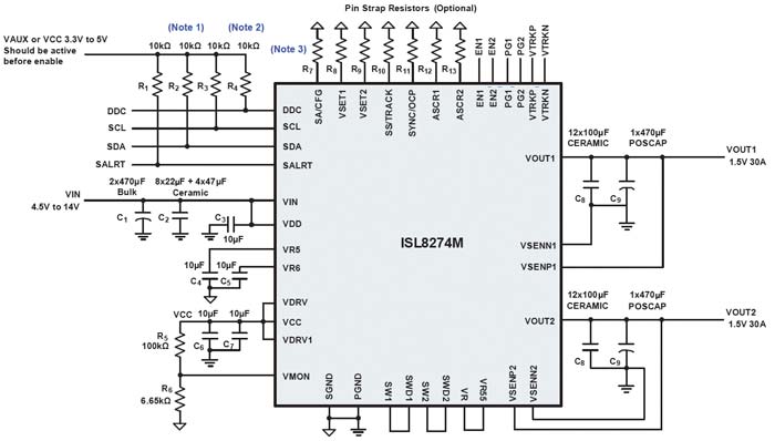
Figure 1. General application circuit of the ISL8274M.
Digital Power Modules Adapt to FPGAs
Analog and digital power modules are both suitable for FPGA power supply applications. However, digital power management provides many additional benefits such as real-time monitoring, digital control with fast transient response, reduced bill of materials (BOM), and simplified design effort. The digital power module solution is flexible and can adapt to the changing FPGA power requirements of lower voltage, higher current and additional rails with less effort. A new voltage rail is easily added to the power management system through the PMBus. Renesas’ proprietary Digital-DC (DDC) communication bus is used to provide a communication channel between power devices, enabling trouble-free communication, sequencing, interleaving, and fault spreading. Today, many digital power modules can achieve excellent output voltage regulation accuracy with the exact set-point reference.
The ISL8274M is a general-purpose step-down digital power module and features PMBus communications and numerous other characteristics that satisfy the requirements for FPGA power supplies. It has two channels, which can operate as two separate power rails for different FPGA parts or connect in parallel to support the same rail with a high current capability requirement. Moreover, the ISL8274M has an internal DDC serial bus that enables communication between other Renesas power devices, allowing easy configuration and implementation of power-up sequence, fault protections, and monitoring. Its general application circuit is shown in Figure 1.
Table 1. Key features of the Renesas ISL8274M digital power module
| ISL8274M Key Features | ||
| • Complete digital power supply • 30A/30A dual-channel output current − 4.5V to 14V single rail input voltage − Up to 95.5% efficiency • Programmable output voltage − 0.6V to 5V output voltage settings − ±1.2% accuracy over line/load/temperature |
• ChargeMode™ control loop architecture − 296kHz to 1.06MHz fixed switching frequency operations − No compensation required − Fast single clock cycle transient response • PMBus interface and/or pin-strap mode − Fully programmable through PMBus − Pin-strap mode for standard settings − Real-time telemetry for VIN, VOUT, IOUT, temperature, duty cycle, and switching frequency |
• Advanced soft-start/stop, sequencing, and tracking − Complete over/under voltage, current and temperature protections with fault logging − PowerNavigator™ support − Thermally enhanced HDA package |
Digital ChargeMode Control Scheme
The ISL8274M uses Renesas’ patented ChargeMode™ control scheme, which has the ability to achieve a fast response when loading the transient with a fixed switching frequency and to support an all-ceramic output capacitor design. Delays are reduced between the error-sampling instant and the moment the PWM is generated using a multi-rate sampling technique and digital filter. This is also an easy compensation control scheme, achieved without the need for extra passive RC components for a compensation loop design as required by an analog module. For any in-system change, new compensation can be easily reconfigured by the PMBus command or PIN-strap setting. A reference design is provided by the manufacturer for the user’s convenience.
Soft-Start with Adjustable Ramping Time
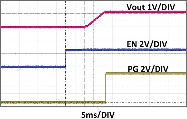
Figure 2. ISL8274M startup performance.
It may be necessary to set a delay from the time when an enable signal is received until the output voltage ramps to its target value. The ISL8274M provides designers with an easy process through the PowerNavigator™ GUI design tool to reset both the delay and ramp times precisely and independently. The ISL8274M also provides pre-bias protection by sampling the output voltage before initiating an output ramp in the event a pre-bias condition exists at the output stage prior to startup. Figure 2 shows the soft startup process, with startup rising time equal to 5ms.
Power Sequencing/Voltage Tracking
A group of power modules for different rails or multiphase operation can be configured to power up in a predetermined sequence. This feature is especially useful when powering advanced processors, such as FPGAs, that require one supply to reach its operating voltage prior to another supply reaching it in order to avoid latch-up. With the ISL8274M, multiple device sequencing is configured by issuing PMBus commands to assign the preceding device in the sequencing chain, as well as the device that follows the sequence.
The ISL8274M integrates a voltage tracking scheme that allows one of its outputs (Channel 1 or Channel 2) to track a voltage that is applied to the VTRKP and VTRKN pins, with no external components required in two optional modes that are based on the specific application.
Various Protection Functions and Monitoring
A full list of protection functions is supported by the ISL8274M, including power input under-voltage/over-voltage (UV/OV), driver voltage UV/OV, two levels of output current under-current/over-current (UC/OC) (average and peak), output voltage UV/OV, and temperature under-temperature/over-temperature (UT/OT). Each protection has both a fault limit and warning limit. The user can set the corresponding fault limit value easily through PMBus commands. There are also different fault response options from which a designer can choose, including hiccup mode. Additionally, the designer can configure the response function through the PMBus command. The ISL8274M is able to monitor a wide variety of system parameters using PMBus commands.
The most complete set of protection functions and monitoring features are provided by the ISL8274M from Renesas. These functions protect the power system operation in a safer, more robust manner and provide increased system design flexibility to the designer.
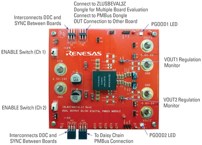
Figura 3. Evaluation board image of ISL8274M.
Design Tools from Renesas
Evaluation Board/User Guide
An evaluation board and detailed user guide for customer testing and evaluation are available for the ISL8274M. A photograph of the evaluation board is shown in Figure 3.
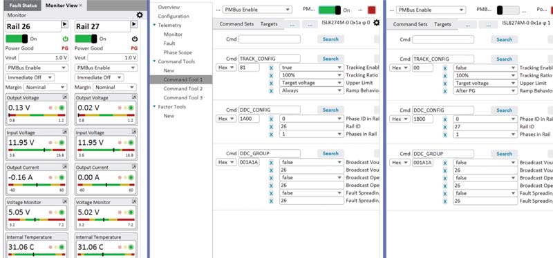
Figure 4. Screenshot of PowerNavigator windows.
PowerNavigator
The PowerNavigator GUI software offered by Renesas will help accelerate the design, testing, finalization, and debugging of your power design. It connects to development boards through PMBus to set various adjustable system parameters and threshold values. The final configuration is simply stored to non-volatile memory. Figure 4 shows an example of the PowerNavigator GUI software windows.
PowerCompass
The PowerCompass tool helps users quickly identify parts that match their specific requirements, set up multiple rails, perform high-level system analysis, and generate custom reference design files. The tool is available exclusively as a web app, from which users can also work offline.
iSim Design & Simulation Tool
Renesas provides a power web-based simulation tool called iSim, which is an easy-to-use, interactive power management and op-amp design tool. iSim allows the user to quickly select supporting components and design and simulate their circuit and system.
Conclusion
The ISL8274M digital power module leverages the Renesas patented ChargeMode control architecture to provides the highest efficiencies with better than 90% on most conversions. It provides a single clock cycle fast transient response to output current load steps common in FPGAs that process power bursts. Their compensation-free design keeps the module stable regardless of output capacitor changes due to temperature, variation or aging. Its power density, high efficiency and fast transient response address demanding single and multi-rail power requirements. Learn more about the ISL8274M: https://www.intersil.com/products/isl8274m
Detailed instructions and video tutorials on the PowerNavigator, PowerCompass, and iSim Design & Simulation Tool are available online and can help the user get started easily:
- https://www.intersil.com/powernavigator
- https://www.intersil.com/en/powercompass.html
- https://www.intersil.com/en/tools/isim.html
About the author: Xiao Li is a Senior Applications Engineer with the Industrial Analog & Power Group at Renesas Electronics Corporation.
Renesas Electronics Corporation