


The majority of the silicon of early A/D converters was analogue, but as new approaches evolved, devices became predominantly digital. This presented different problems for the PCB designer, but in many cases PCB layout practices have not changed significantly. This article will look at the layout techniques needed for A/D converters using successive approximation register (SAR) and Sigma-Delta topologies.
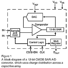
SAR A/D converters were originally bipolar devices with an R-2R ladder configuration. More recent designs have used a capacitive charge distribution topology and have been implemented in CMOS. The system layout strategy for these converters has not needed to change, except for those converters with higher resolution.. Layouts for these devices need more care, to prevent digital feedback from the converter’s output interface. Most of a SAR converter is analogue. A block diagram of a 12-bit CMOS SAR converter is shown in Figure 1.
The sample/hold, comparator, most of the digital-to-analogue converter and 12-bit SAR are analogue. The remainder is digital. Most of the current drawn by this converter supplies the internal analogue circuitry. The only digital current coming from the device is the small amount of switching that occurs in the D/A converter and at the digital interface. The ground and power connections to these converters are usually made via several pins. However, the pin names can be misleading. They are not intended to describe the system connections to the PCB, but to indicate how the digital and analogue currents come off the chip. Once we understand this, and know that the majority of the chip is analogue, it is sensible to connect power and ground pins to the analogue planes. Example pinouts for 10-bit and 12-bit converters are shown in Figure 2. With these devices, provided the package has sufficient pins, the ground is usually directed off the chip with separate analogue and digital ground pins – AGND and DGND. These separate grounds improve the chances of getting good and repeatable accuracy from the converter. When implementing the PCB layout using these chips, the AGND and DGND should be connected to the analogue ground plane. The analogue and digital power pins should be connected to the analogue power plane, or at least connected to the analogue power train with proper by-pass capacitors as close to each pin as possible. The power supply strategy should be to connect all grounds, positive supply and negative supply pins to the relevant analogue plane. In addition, the ‘COM’ pin or ‘IN’ pin associated with the input signal should be connected as close to the signal ground as possible. SAR converters with high resolutions, such as 16 or 18 bits, present more layout constraints. It is much more important to separate the digital noise from the quiet analogue planes on the printed circuit board. These devices are often interfaced to a microcontroller, in which case external digital buffers should be used, in addition t the internal buffers that are usually incorporated at the digital output of the converter. A suitable layout for this type of system is shown in Figure 3. In precision sigma-delta A/D converters, the silicon area is predominately digital. This difference originally convinced designers that they should separate the digital noise from the analogue parts of the circuit by using different power and ground planes. This is not actually the best way, especially for devices .in the 16- to 24-bit range. High-resolution sigma-delta converters with a 10Hz data rate have a clock frequency as high as 20MHz. As with the SAR converters, the AGND and DGND pins should be connected to the same ground plane, and the analogue and digital power pins should preferable be connected to the same power plane. A ground plane is essential, so a doublesided board is needed at minimum. The ground plane should cover at least 75% of the area of the board, and prefer ably more. The ground plane reduces grounding resistance and inductance as well as provid ing a shield against electromagnetic inter ference and radio-frequency interference. If circuit interconnect traces must be put on the ground-plane side of the board, they should be as short as possible and perpendicular to the ground current return paths. By following the above techniques, designers will reduce the problems often encountered with A/D converters. By making use of the low-noise nature of the analogue power and ground planes, in some cases in conjunction with additional buffering, it is possible to keep noise to a minimum.
www.microchip.com
euro.enquiry@microchip.com