


 While analogue and digital signals may behave quite differently, they often have to work alongside one another in electronic systems. Signals originate in the real world and they need to move back into it for humans to perceive and interact with them. This is where data converters − either analogue to digital converters (ADCs) and digital to analogue converters (DACs) − come in, often accompanied signal conditioning to prepare signals for the next stage of processing.
Analogue waveforms vary continuously in frequency and amplitude over time, represented by a potentially infinite set of values. The sounds we hear and the words vocalised when we speak are analogue. Images and video are analogue at their source too, translated into vision by the sophisticated analogue sensors that are our eyes. Measuring our heartbeat or tracking our movement both entail capturing analogue signals and subsequently processing them.
In contrast, digital information is represented by discrete time and amplitude quantized signals using digital bits in the binary format. This digital language lends itself to efficient processing and long-term storage of data. It is, as a consequence, used extensively in computing and telecommunications systems.
Electronic hardware will always require interfaces that translate signals from the analogue domain into the digital domain, and vice versa. ADCs and DACs are thus fundamental components for engineers to make use of. Consider designing a smart climate control system for a vehicle. Engineering teams faced with this task will need to read multiple analogue temperatures from sensors in different passenger zones throughout the cabin, as well as from external sensors. ADCs will be employed to convert these analogue values into a binary representation − with discrete steps that can then be processed by the system microcontroller unit (MCU). The MCU will combine this data with commands and settings entered by occupants via a human machine interface (HMI). The analogue temperature values derived from the vehicle occupants (as well as the physical HMI commands) will again be converted to digital signals by an ADC. The digital signal data that has been amassed will then be utilised by the MCU in order to maintain a stable environment. DACs may be used to convert digital signals back to analogue ones to provide feedback to the HMI. The binary code would be completely unintelligible to the vehicle occupants otherwise.
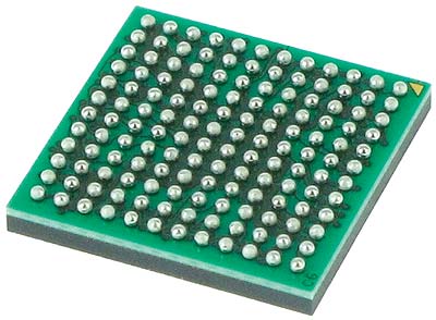
Figure 1: Texas Instruments’ ADC12DJ3200 ADC
Technological progression within the data converter arena
Incremental innovations in data conversion over the past few decades have not only enabled performance advances (benefiting everything from cellular communications and medical imaging to consumer audio and video), they have also helped to spawn entirely new applications. Ever rising demand for broadband communications (both wireline and wireless), high performance imaging applications (from medical/scientific imaging to industrial inspection), plus the emergence of AR/VR, facial recognition, etc., have resulted in increased focus on high-speed data conversion.
Converter ICs that are capable of handling signal bandwidths beyond 1GHz are becoming more and more commonplace. A range of different mixed signal architectures have been employed to achieve these cutting-edge speeds, each with particular operational advantages. The greater processing power and data throughput enabled by shrinking process technologies, delivering smaller transistors that can switch faster (and at lower power), leads naturally to faster conversion. As a result, broadband signals expand their bandwidths (often to the spectrum limits set by physical laws), imaging systems look to handle more pixels/s − so as to render higher resolution image content faster. As systems are re-architected to take advantage of this extreme processing horsepower, there is an emerging trend toward multi-channel data converters, and even software-defined systems.
Rather than the conventional approach of doing much of the signal conditioning work in the analogue domain when identifying, filtering and amplifying a radio station signal of interest (before taking the signal into the digital domain), a multicarrier architecture approach might digitise the entire spectrum, and then use digital processing to identify, select and recover signals of interest. This requires more sophisticated circuitry, but offers important advantages, enabling simultaneous recovery of multiple stations. Effectively, a wideband digitiser combined with a powerful processor, plus a data converter with heightened speed and performance, forms a software-defined radio that can recover any kind of signal – the signal processing equivalent of virtualisation.
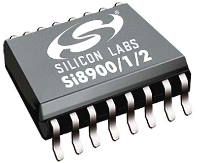
Figure 2: Silicon Labs’ Si890x ADC
Analog Devices (ADI) recently introduced the first in a new line of RF converters designed for elevated bandwidth applications, such as 4G/5G multi-band wireless communications base stations, multi-standard production test systems and defence electronics. Based on 28nm CMOS technology, the AD9213 provides a strong combination of speed, bandwidth and dynamic range. Featuring higher parametric performance, greater Nyquist bandwidth and RF sampling capabilities at higher analogue input frequencies than conventional RF ADCs, it allows digitisation of RF signals up to 7GHz. Designed to enable the next generation of software-defined systems in avionics, instrumentation and communications, it drives greater system integration and reduced power consumption.
The AD9213 provides aerospace and defence engineers with the ability to process larger sections of spectrum in electronic surveillance applications, as well as increased resolution and longer range in radar systems.
High-density phased-array radar systems, 5G test systems and satellite communications all demand increased data throughput, ramped-up bandwidth and lower power, while often having PCB footprint constraints too. The wideband ADC12DJ 3200 ADC from Texas Instruments delivers an ultra-fast sampling rate of 6.4GSPS at 12-bit resolution. Thanks to its high analogue input frequency range, with direct RF sampling up to 10GHz (covering the L, S and C-bands and extending into the X-band), it enables simplified system architectures and provides enhanced frequency agility, while reducing filter complexity − which in turn saves board space and keeps component count low.
For engineers designing continuous monitoring solutions for wearable health and fitness applications, Maxim offers a complete electrocardiogram (ECG) and bio-impedance (BioZ) analogue front-end (AFE). Measuring heart rate, respiration and arrhythmias, the MAX30001 is small and power efficient enough to be incorporated into bio-sensing clothing to monitor and track health metrics 24/7. This clinical-grade device features high-resolution data converters, delivering 15.9-bits effective number of bits with 3.1μVPP (typical) noise for ECG measurements and 17-bits effective number of bits with 1.1μVPP (typical) noise for BioZ measurements.
Designed specifically for the demands of mains line monitoring, Silicon Labs has introduced the industry’s first isolated 10-bit ADCs. The devices in the Si890x family employ the company’s patented CMOS-based digital isolation technology. Integrating both ADC and isolation functions provides a much smaller and thinner footprint solution than conventional transformers would be able to. Each ADC input features a 3-channel analogue multiplexer, which enables a single Si890x to monitor up to three different signals (typically AC mains voltage and current, along with the third channel serving as a spare).

Author: Mark Patrick, Mouser Electronics
Mark joined Mouser Electronics in July 2014 having previously held senior marketing roles at RS Components. Prior to RS, Mark spent 8 years at Texas Instruments in Applications Support and Technical Sales roles and holds a first class Honours Degree in Electronic Engineering from Coventry University.
Mouser Electronics | www.mouser.com
![]()