Increased processing density in high-end data server designs with the cramming of more and more silicon on to PCBs continues to have an impact on power supply systems. For example, power per board demand from ICT (Information and Communications Technology) servers has increased from 300W in the early 1980s to more than 1kW today – and it is expected that power per board of 3 to 5kW will be required by the end of this decade. In addition, equipment will be required to occupy less space, implying a higher overall power density. Current DC/DC power converter technologies are not adequate at these levels of power and although a 1kW converter can be accommodated in a quarter-brick format today, the deployment of 3D packaging, the highly integrated embedding of components and enhanced thermal management technologies will be needed to produce, for example, a 1kW converter in an eighth-brick format.

Author: Patrick Le Fèvre, Marketing and Communication Director at Ericsson Power Modules
Three Dimensions
Today’s DC/DC power converter bricks still widely use a planar and two-dimensional PCB construction, but applications that require smaller footprints, lower profiles and reduced parasitic impedances are driving demands for high-density 3D packaging. While its use is limited in high-power bricks today, there are many possibilities in embedding both active and passive components via methods such as chip stacking, package stacking and component embedding through over-moulding. These can offer significant gains in footprint reduction, enhanced cooling possibilities and the positioning of drivers in close proximity to switching devices. This will enable improvements in performance and efficiency by minimization and the precise control of interconnect parasitic impedances in high-frequency switching circuit designs. Subsequent 3D assembly of additional components will further contribute to reducing footprint and also the size of magnetic components.
Components
Switching frequencies for high-power converters are generally optimized for operation of approximately 500kHz or below, but to enable size reduction and an increase in power density, a switching frequency of 2MHz and above will be necessary to minimize the magnetic physical volume. The recent availability of wide-band-gap (WBG) semiconductor components such as GaN and GaAs based switching FETs, ideally operating at higher frequencies in excess of 5MHz, is certainly an enabler for higher switching frequencies. In fact, new topologies may even increase switching frequencies well into the 10MHz range, thereby driving requirements for packaging with reduced parasitic components, which can be achieved using 3D integration techniques.

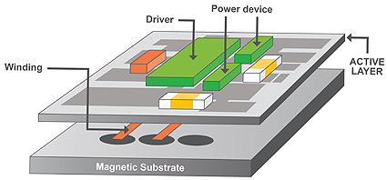
However, higher switching speed is dependant on the availability of low-loss high-frequency magnetic materials, leading to power transformer and inductor solutions that are suitable for high-volume production. There are several viable technology paths to higher-frequency miniaturized and integrated magnetic components including advanced magnetic-core designs and core materials, as well as air-core designs that are not dependent on core material characteristics. This means that there is also flexibility in production methods and the possibility to use different 3D integration techniques such as embedded windings in multi-layer PCB and multi-layer ferrite substrate with integrated active Cu layers (see figure 1).
While these techniques are largely limited to lower power converters, further improvements in core materials and expansion into products with increasing output current will be enabled by improved processes for magnetic materials. In addition, the ultimate goal of integrating the magnetics within the semiconductor wafer is possible in the future.

Thermal Management
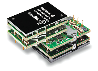
Power density, in terms of watts per cm3, is now an order of magnitude higher than it was 15 years ago. And the latest power bricks (see figure 2, as an example) can place some very high demands on efficient internal thermal management.
Clearly, it is essential to ensure components in high-power-density bricks are cooled – usually via mechanisms such as conduction and convection – for operation at reasonable temperatures, otherwise semiconductor device performance and system reliability may be compromised. Component power dissipation (Pd, comp) and component junction to case thermal resistance (Rth, J-C) for each critical component becomes extremely important as they determine the actual junction temperature that limits the DC/DC converter’s thermal performance. The temperature difference between the component junction (or core) and case can be calculated using: D(Delta)TJ-C = Pd, comp × Rth, J-C
Advanced cooling technologies and techniques that improve the thermal performance of new and emerging 3D packaging assemblies that aim to double power density (to 75W/cm3 or 1200W/in3) are absolutely crucial and ultimately will determine the feasibility of higher power densities.
However, many standard components are not suitable for high-density or 3D designs due to insufficient thermal performance. And other thermal design challenges will include high-current distribution, assembly on 45-layer boards for example, and the inadequacy of even greatly enhanced traditional cooling techniques such as existing air-blown convection.
Over-moulding is likely to continue as a technology used for improving thermal performance, but it is also clear that thermally enhanced packaging for all power components, including magnetic components and capacitors, will be required to allow cooling from at least two opposite surfaces, together with the use of improved thermal materials, processes and cooling techniques.
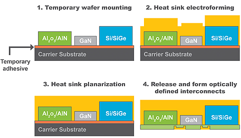
As shown in figure 3, instead of mounting power components on a PCB with die attach or thermal interface material, the components are held on a temporary carrier and a heat sink is electroformed around them.

Components of various sizes and thicknesses can be integrated on the same board, called an Integrated Thermal Array Plate (ITAP).
When the carrier is removed, the bottom and top surfaces of the components are co-planar and facilitate a defined and optimised thermal connection. Improvements in thermal resistance of up to 50%, (i.e. 50% higher power dissipation for a fixed TJ) can be achieved compared with conventionally packaged components with epoxy or solder attach.
Through-Silicon-Vias (TSV) will also be a potential solution in stacked chip solutions in combination with liquid cooling techniques, and experimental results have indicated the potential of a 50% improvement in thermal performance.
The replacement of solder and thermal grease with sintering in assemblies using Direct Bond Copper (DBC) technology is another technique that could significantly improve thermal performance. Other potential cooling techniques include both liquid conductive cooling of certain high-power components and forced-air convection cooling of medium- and low-power dissipating components.
And the use of passive liquid cooling technologies such as heat pipes is likely to become more widespread to deal with local hotspots.
Doubling Power Density
New developments in 3D packaging and chip-scale IC will continue on, but will also include the integration of power magnetics that will increase the power levels far beyond today’s non-isolated converters. The use of planar magnetics is already widespread and the power converter assemblies will probably be over-moulded to improve thermal performance.
However, these developments cannot be driven by the DC/DC power converter industry alone, and support from makers of semiconductors and other power components will be essential with a supply chain that offers standardized requirements and qualification tests.
Experimental results and full-scale production show the potential of achieving double the power density combined with thermal management solutions for keeping the component core temperatures within specified levels for reliable operation, making it easily possible to foresee a 1kW eighth-brick in the near future ■

Ericsson Power Modules
www.ericsson.com/powermodules


