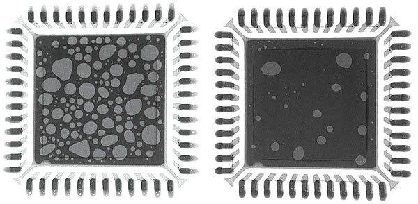
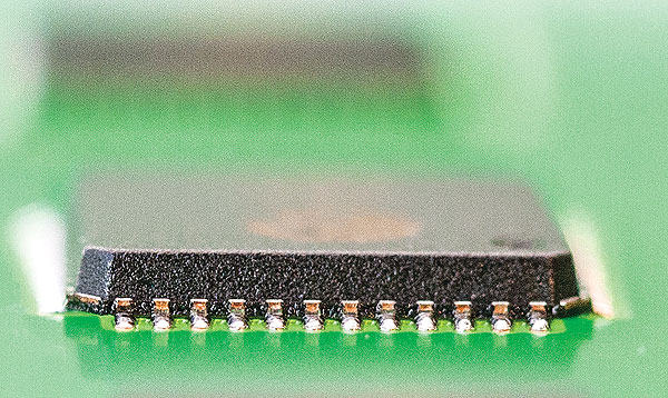
Void formation under components with large soldering planes and low stand-off heights, such as QFN components, is a well-known phenomenon. The use of this type of components is on the rise, giving many designers, SMD line operators and quality control staff ever growing headaches to meet IPC criteria. This article focuses on a novel approach toward void reduction.
Introduction
The mechanism behind the formation of voids in a solder joint has been the subject of study for many years. A number of void types and forming mechanisms have been identified. Most notable are macro voids, where the main contributor to the void formation appears to be the soldering chemistry of the solder paste.
Micro voids, shrinkage voids and Kirkendall voids are also well known and documented void types, but fall outside the scope of this article. Many techniques to reduce void formation have been established over the years.
Adjusting the solder paste chemistry, the reflow profile, the component, PCB and stencil design or finish, are some of the optimizing tools that are actively being used in the field today.
Even machine manufacturers are jumping on the wagon by offering solutions to reduce voids by ways of a frequency sweep or vacuum technology.
There is, however, another very important, parameter that defines void formation : the soldering alloy.
The soldering alloy: an unusual suspect
The main contributor to void formation is and has always been thought to be the solder paste flux. Designing a solder paste flux that actively works on reducing voids seems to be the right way to go, since about 50% of the flux paste will evaporate during the reflow process, actively generating voids.
Because of this focus on the solder paste flux however, investigations on void formation differences between soldering alloys have always been flying under the radar. Until now.
Void level determination
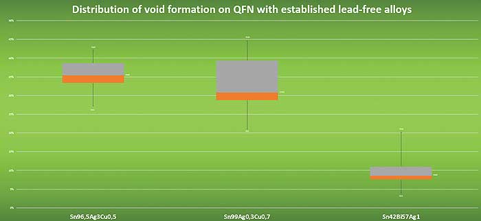
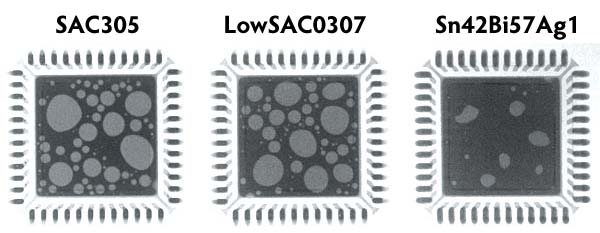
A baseline void formation percentage was established with standardly available soldering alloys, such as SnAg3Cu0,5(SAC305), SnAg0,3Cu0,7 (LowSAC0307) and Sn42Bi57Ag1. The same solder paste chemistry was used for all tests described in this paper.
To level out differences between PCB finishes, tests were performed on 3 commonly used finishes in the field: OSPCu, ENIG (NiAu) and I-Sn.
To have sufficient void generation, a stencil of 120µm was used without any pad reduction.
60 Sn-finished QFN components for each paste were reflowed using a standard ramp-up reflow profile, suitable for each specific soldering alloy.
Each component was x-rayed and the void level of the ground plane was used for determining the void percentage. Void percentage is calculated as the area of voids compared to the area of the ground plane surface.
Individual void size was not taken in consideration.
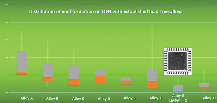
The test results show rather poor results for SAC305 and LowSAC0307. Better results were obtained with Sn42Bi57Ag1.
Alloy optimization
Based upon these test results, a research project was started to determine the optimal soldering alloy in perspective of voiding performance. TGA analysis and X-Ray analysis were used for this purpose. Further parameters, such as reflow profile, yield strength, pasty range, elongation and usability in other processes were taken into consideration as well.
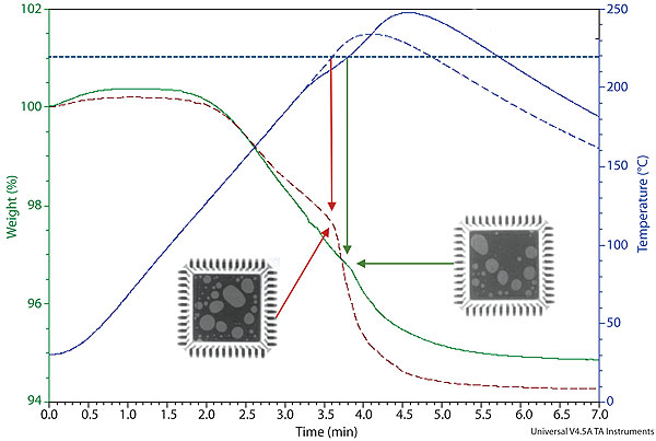
The strategy of development involves starting with the standard lead-free soldering alloys and adjusting them with e.g. Sn, Bi, Ag, Zn, Cu, … As this quickly results in numerous candidate alloys TGA analysis was used as an initial selection tool. With TGA analysis, the evaporation of the flux paste chemistry in combination with a certain alloy and reflow profile can be monitored. A smoother evaporation curve means lower void formation. From this research 8 Prototype soldering alloys were chosen for further investigation.
Super-8
The 8 prototype soldering alloys were subjected to the same test setup as the initial reference testing. This means soldering QFNs with each solder paste on different PCB finishes and analyzing real voiding performance with X-ray. The initial test results showed significant reduction of the void levels when compared to the standard SAC305, LowSAC0307 and even Sn42Bi57Ag1.
Test alloy G resulted in lowest voiding values in combination with the narrowest spreading of the results.
This alloy was selected for further mechanical reliability testing.
Together with its low voiding properties it also showed good shock and vibration resistance in combination with better thermal cycling properties than SAC305.
Furthermore, beside reflow, the alloy proved also to be suitable for wave and selective soldering. Alloy G was chosen for commercialization under the name LMPA™-Q.
Conclusion
A serious decrease in void formation was obtained with the adjusted soldering alloys when compared to the market standards SAC305 and LowSAC0307.
Furthermore, the ultra-low voiding soldering alloy LMPA™-Q performs better in thermal cycling & vibration resistance when compared to most of the soldering alloys used on the market today.
 Bio
Bio
Ralph Lauwaert has more than 10 years of experience in the field of electronics manufacturing. At the manufacturing company of soldering chemistry, Interflux® Electronics NV in Gent (B), he got the opportunity to give world wide support to the Interflux subsidiaries, customers and distributors.
Many years of hands-on experience in a wide variety of applications, processes and their parameters created the basis for an expertise in analyzing and solving reliability problems.
Want to know more? ▶▶▶ www.lmpa-q.com
For more information, please contact:
Eng. Ciprian Varga, Technical Director
![]() Comet Electronics | www.comet.srl.ro | office@comet.srl.ro
Comet Electronics | www.comet.srl.ro | office@comet.srl.ro
Tel.: +40 (0) 21 243 2090 | Fax: +40 (0) 21 243 4090


