


A reference design is proposed by Alex Dumais of Microchip Technology Inc.
The combination of the flexibility of digital power control, with the improved efficiency of Inductor, Inductor, Capacitor (LLC) resonant converters, can help telecoms and other medium to high power applications to minimise energy consumption and cooling equipment operating costs.
Digital control offers significant design advantages such as a high level of flexibility coupled with high performance and high reliability, whilst LLC resonant converters increase efficiency by significantly reducing the power dissipated by the MOSFETs within a DC-DC converter.
Together, these technologies can help companies to meet the new efficiency targets set by initiatives such as the ENERGY STAR Data Center Energy Efficiency Initiative and the 80 PLUS® Initiative. The ENERGY STAR Data Center Energy Efficiency Initiative targets information technology (IT) equipment and infrastructure, uninterruptible power supplies (UPS) and other equipment which are responsible for high levels of energy consumption.
The 80 PLUS® Initiative addresses the fact that many power supplies time operate spend considerable time operating at loads which are far below the level at which that achieve the greatest efficiency. This initiative stipulates that 80% efficiency should be the minimum for a 115V power supply operating at 20%, 50% and 100% of its rated load. Platinum, Gold, Silver and Bronze ratings can be awarded when a supply exceeds these efficiency targets. In order to achieve the Bronze rating, for example, a 230V supply should achieve 81% efficiency at 20% and 100% of its rated load and 85% efficiency at 50% of rated load.
Further impetus for increasing power efficiency is coming from end-users who are including the requirement for power supplied to be certified by these initiatives within their purchasing contracts.
For the designer, energy-saving power-supplies can be realised by combining the efficiency of an LLC resonant converter, with the advanced digital control offered by digital signal controllers (DSCs) such as Microchip Technology’s dsPIC® family. These low pin-count DSCs offer powerful digital signal processing (DSP) capabilities in addition to intelligent power peripherals optimised digital power control.
The basics of resonant converters
Operating a converter in resonant mode, at the point where the impedance between the input and output of the circuit is at its minimum, provides improved efficiency. For example, the power dissipated by the MOSFETs in an LLC resonant converter can be significantly reduced by supplying the MOSFETs with either a sinusoidal voltage or a sinusoidal current, and switching in close proximity to the zero crossing of the sinusoidal voltage or current.
Switching the MOSFET when the drain-to-source voltage is near zero, Zero Voltage Switching (ZVS), and transitioning from one MOSFET state to another while the current through the switch is zero, Zero Current Switching (ZCS), minimises MOSFET switching losses. This soft-switching approach also reduces noise in the system and provides improved electromagnetic interference (EMI) performance. For high-voltage, high-power systems, ZVS would be the preferred topology.
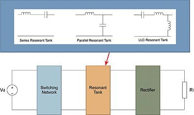
In a resonant-switch converter, the sinusoidal voltage or current is generated by reactive elements such as capacitors and inductors. The three main classes of resonant converters are: series resonant converter (SRC), parallel resonant converter (PRC) and a combination of the two, the series-parallel resonant converter (SPRC). Figure 1 shows the high-level resonant converter block diagram and the three types of resonant-tank circuits.
In the series resonant converter, the load is connected in series with the tank’s inductor and capacitor. The gain from the resonant tank is ≤ 1. While the SRC can operate at no load, its output voltage cannot be regulated. For ZVS, the circuit needs to operate above resonance in the inductive region. At low line voltage, the SRC operates closer to resonant frequency.
In the PRC, the load is connected in parallel with the resonant capacitor. The PRC can operate at no load output and, unlike the SRC, its output voltage can be regulated at no load. For ZVS, the PRC also needs to operate above resonance in the inductive region. Similar to the SRC, at low line voltage, the PRC operates closer to resonant frequency, however, the PRC differs by having high circulating currents. The series inductor and parallel capacitor provide protection against short-circuits.
In an SPRC, the tank circuit is a combination of the series and parallel converters and can be either a LCC or LLC configuration. Similar to the SRC and PRC, a SPRC LCC design cannot be optimised at high input voltage. As a result, the preferred alternative for many applications is an LLC, shown in Figure 1.
The LLC converter can operate at resonance, at nominal input voltage, and is able to operate at no load. In addition, it can be designed to operate over a wide input voltage.
Both zero-voltage and zero-current switching are achievable over the full operating range.
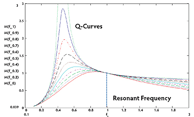
The performance of a resonant converter is measured by several parameters. The quality factor (Q) of a resonant circuit is a dimensionless parameter that describes the amount of dampening in the circuit. It is defined as the ratio between the power stored and the power dissipated in the circuit. A higher Q indicates a narrower bandwidth for the resonant tank.
Quality is a key parameter in the tank circuit’s gain, which is also called the voltage conversion ratio or M. By considering the families of M curves that are generated when varying either l, the normalised frequency, or Q, it is possible to obtain an indication of a resonant converter’s performance before all the parameters have been computed.
M is defined as:
M(fsw) = f ( fn, l, Q)
Where:
fn = normalised frequency, f/fr
l = the inductance ratio, Lr/Lm
Q = quality, a function of the output
impedance
As shown in Figure 2, the LLC circuit for Q as a parameter has two resonant frequencies: one due to the presence of Lr and Cr, the series inductor and capacitor at 0.5; and the second one due to the parallel inductor, Lm. Lr and Cr have a resonant frequency at fn = 1 (fr) and Lm + Lr and Cr have a resonant frequency at fn ~ 0.5.
Different operating modes of the LLC include: at resonance; below resonance; or above resonance. At resonance, the MOSFETs are switched at the resonant frequency within a very narrow timing window, as determined by the selected components, to produce very low losses.
Below resonance, the circuit behaviour is similar to that at resonance, but the tank current is limited by the magnetising current for a portion of the cycle. If MOSFETs are used for synchronous rectification in the secondary instead of diodes, the gates must be turned off at the correct time. This usually requires a current-sensing technique, such as measuring the voltage drop across the MOSFETs.
Above resonance, instead of being limited by the magnetising current, the tank current is higher than the magnetising current. In this region, the synchronous switches can be turned on and off at the same time as the primary switches to simplify control.
Since zero-voltage switching is used, LLC resonant supplies have inherently low electromagnetic and radio interference.
Digital control topology for increased efficiency
Full digital control of the power-conversion and system-management functions of the LLC resonant converter can easily be implemented using the latest generations of DSCs.
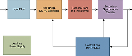
In addition to the components and sections shown in Figure 1, an LLC circuit includes a DC input, switch network, LLC resonant tank, transformer, rectifier, filter and load. A digitally-controlled feedback loop for an LLC resonant converter, used in a telecoms application, is shown in Figure 3.
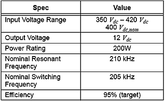
In telecoms, the LLC converter is widely used as the DC/DC converter following a Power Factor Correction (PFC) circuit in an AC-DC system. The typical PFC output voltage of around 400V can be directly fed into the LLC converter. The wide input range allows the use of smaller bulk capacitors. The design specifications are summarised in Table 1.
With 40 MIPS performance and intelligent power peripherals a dsPIC33FJ GS provides the digital computing power in the resonant converter. The peripherals include high-speed 16-bit PWM with features which include 1 ns period resolution and phase-shiftable outputs.
The reference design’s switching circuit uses a half-bridge topology so the half-bridge voltage swings between 0V and Vd of 400 Vdc nominal. The resonant tank circuit comprises a capacitor, inductor, and the magnetising inductance of the isolating transformer to reduce system cost by eliminating the need for an external inductor. This design can also use the transformer’s leakage inductance as the second inductor and eliminate another external inductor for additional cost savings.
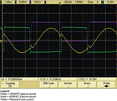
If correctly tuned to the switching frequency, the resonant tank presents finite impedance to the fundamental frequency and very high impedance to all other harmonics. The impedance of the tank causes a phase shift between the voltage and current, which allows ZVS to occur. Figure 4 shows the ZVS of the primary MOSFETs.
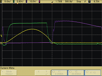
The secondary side has been designed using a synchronous rectifier, instead of diodes, to reduce conduction losses at the secondary. This reduces both the forward resistance (Rf) and the losses due to the diode forward voltage. Figure 5 shows the switching waveform for the synchronous rectifier.
For synchronous rectification, the digital control initiates the switching of the FETs without requiring current-sensing circuitry on the secondary.
This results in improved efficiency and reduced cost over a full-wave rectifier design. Figure 6 shows the efficiency over the load current range:
The efficiency of the LLC at two different input operating voltages shows its
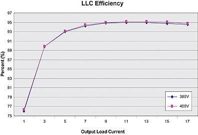
insensitivity to input voltage. Over 80% efficiency is achieved with an output load current below 2A, whilst, at higher loads, the maximum efficiency is 95% and extremely flat from 7 to 17A. Additional benefits include enhanced flexibility for the compensator design, by using the DSC to implement soft-start for duty-cycle control.
Since the power-conversion control is implemented with easily reprogrammable software, it provides designers with ability to easily modify or adapt their design, or add new, cost-effective and value-creating features. The precision of the digital control also improves the power supply’s reliability.
Summary
The combined advantages of LLC resonant converters and digital control via DSCs enable designers to increase energy efficiency for DC-DC converters for telecoms and other
medium to high-power applications. Whilst LLC resonant converters can reduce power losses, digital control increases the inherent flexibility efficiency and reliability of the converter. The proposed reference provides a basis from which designers can to achieve higher efficiency converters and a faster time to market.

Microchip Technology
www.microchip.com
Further reading: A more detail description of the reference design using the dsPIC DSC is available in Microchip Technology’s AN1336 application note: DC/DC LLC
RESONANT CONVERTER Reference Design
Note: The Microchip name and logo, and dsPIC, are registered trademarks of Microchip Technology Inc. in the U.S.A., and other countries. All other trademarks mentioned herein are property of their respective companies.