


In the best numerology-style, this article will list the 10 top reasons why embedded control engineers (are going to) love this little and inexpensive 8-pin microcontroller.
The article presents each point as a solution to a very specific problem that presents itself to the budget-conscious, savvy LED driver designer.
Introduction
The PIC12HV752 is a small and inexpensive mixed signal microcontroller designed specifically to please the LED lighting designers.
To be more specific, this class of engineers is looking for new and innovative
Solid State Lighting (SSL) solutions to obtain higher energy efficiency. They
also want to help their companies differentiate by “adding intelligence to lighting.” Regardless of how they plan to achieve it, by providing communication capabilities, advanced sensing, touch inputs or just more flexibility, the key new requirement is the presence of a “brain” in the form of a little Flash based microcontroller.
Unfortunately (or is it fortunately?), since these applications have the potential of running in really high volumes, there is always an extreme attention to the total cost of the solution; and more often then not its size. It shouldn’t come as a surprise that all of the features in the following 10 quick points eventually translate into a significant cost AND size reduction of the overall circuit.
For simplicity, most of the considerations in this article will refer to a buck or fly-back converter topology. However, the experts among you will be able to quickly relate to their (more advanced) topology of choice. Let’s get started!
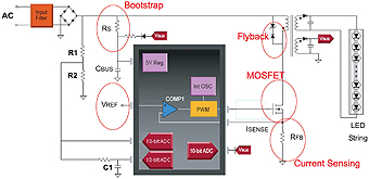
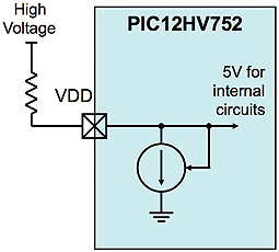
#1 Direct High Voltage Supply
The first thing that comes to mind when thinking of adding a microcontroller to what otherwise could be a simple (analog) dc/dc converter circuit is that you know how finicky these MCUs can be about their own power supplies. You will be glad to hear that with the PIC12HV752 you won’t need to worry about providing a nicely regulated 5V rail. The “HV” piece of the part number was the giveaway, as this device incorporates an on-chip shunt regulator. You can simply place a single resistor in series and hook it straight up to a high-voltage input source. The shunt (operating similarly to a Zener diode) will adjust the amount of current absorbed, as necessary, to allow a voltage drop on the resistor sufficient to guarantee that no more than 5V (±10%) will ever be present on its (Vdd-GND)
terminals.
There is a minimum amount of current that is required to produce a nicely regulated supply: 1mA will do, over the entire temperature range from -40 to +85°C. Other than that, you will be free to use Ohm’s law to determine the smallest resistor necessary, as well as its power.
To ensure that no other external components will be required, the PIC12HV752 includes a power-on reset circuit for proper power up sequencing and a brownout detect circuit to guarantee safe operation when power is cycled.
#2 Monitoring Supply Voltage
Beside the power-on and power cycling conditions, there is a number of reasons why you will need an absolute voltage reference.
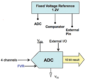
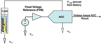
That’s why the PIC12HV752 does include a Fixed Voltage Reference (FVR) with a 1.2V nominal output that can feed directly, without need for external connections, into a 10-bit Analog to Digital Converter (ADC) input channel, and/or an analog-comparator input. This makes it possible for the microcontroller to compare its Vdd to an absolute voltage, which is useful either when a battery power supply is applied, to detect a low battery condition, or in a flyback application to help regulate the voltage output of a secondary supply designed to relieve the shunt regulator (see #1) after a brief initial bootstrap. The latter provides an increase in the overall efficiency of the circuit for a very modest computational cost.
#3 High(er) Frequency Operation
The analog-comparator module provided inside the PIC12HV752 is not the typical device you would expect in your everyday microcontroller. This one is capable of better than 30 ns response time, which is definitely what you want when you need it to control the peak current through your buck converter, operating at speeds up to 500KHz. Most low-cost DC/DC converters will actually stop far short of that limit, and will happily operate between 150-250kHz for the best cost/size compromise.
Some of you will certainly find interesting the option to switch the comparator to a low(er) power mode, where power consumption is traded for speed. In fact, bringing the response time in the 200ns range, the low- power mode provides a significant reduction in the power consumption of the module. This is a valuable option when using the comparator only as a voltage threshold detector in alternative applications; possibly battery operated.
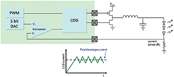
#4 Reducing Sensing Losses
Designed to work in conjunction with the comparators, in a typical buck or flyback converter topology, the PIC12HV752 offers a 5-bit “Limited range” DAC module, with all the proper internal connections to operate as a peak current detector in the
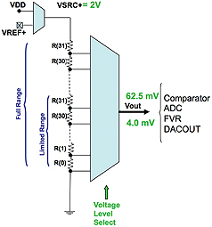
feedback circuit.
Now, if you think that 5 bits might not be adequate for all but the most rudimentary regulation applications, let me explain how this module really operates. For efficiency reasons, the way you detect the current (peak) is by applying the smallest possible series resistor to your load (the LED string). To be realistic, you are looking at a resistive value that provides a few hundred (300) mV feedback. More would be a waste of energy; less would get you in trouble with a poor signal-to-noise ratio. If this signal is applied to one side of a (fast) comparator while the DAC is connected to the other side to set the trip point, the DAC module should provide the maximum resolution specifically in the range between 0 and 300mV. This is exactly what the PIC12HV752 “Limited range” mode operates, providing you with the effective resolution that a 9-bit DAC would (10 mV@5V), but without the cost.
#5 Reducing Switching Losses
Synchronous switching topologies are used in DC/DC converter designs to increase the efficiency (and reduce the so-called switching losses) when the output voltage is relatively low (short strings or single LED).
Essentially, the forward-voltage drop on the “flyback” diode, present in all buck and boost topologies, can be seen as a source of losses. By replacing it with a second active element, we can reduce such losses at the cost of an additional
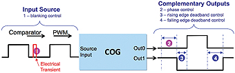
MOSFET and a minimum of circuitry to drive it with the proper (complementary) timing. In fact the PIC12HV752 can make this option really simple to adopt, as the output of the comparator (or the PWM module) can be fed into a small module, known as the Complementary Output Generator (COG), which will provide two complementary output signals ready to drive the MOSFET pair.
The COG module offers additional control over the two output signals, to provide the so called dead-band; a measure that prevents the capacitance of the two MOSFET gates to produce a dangerous cross-bar effect (shoot through).
In reality, there is much more the COG can do to ensure safe control of the synchronous outputs, including:
• Input blanking, to avoid noise on the current feedback and produce multiple commutations
• Phase delay, to stabilize the system without requiring external compensation networks
• Selectable rising-and falling-edge source inputs (PWM, comparator, pin)
• Independent rising-and falling-edge dead-band control
• Selectable shutdown sources
• Auto-restart enable
• Auto-shutdown pin override control
All of these features provide flexibility to help you achieve the ideal compromise between component count, cost and efficiency.
#6 Driving MOSFETs
Among the few components required to assemble a complete DC/DC converter, there is always at least one (power) MOSFET device. PIC® microcontrollers are notorious for their strong output sink and source performance (25mA), but ensuring that a MOSFET is kept out of the linear region requires more.
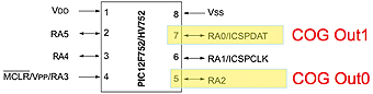
MOSFET drivers are ubiquitous and not particularly expensive, but this is always a relative consideration. The PIC12HV752 does its best to help you reduce cost by providing 50mA strength (sink and source) on two selected I/O pins (corresponding to the two outputs of the COG, of course). While these values are a far cry from the Amperes provided by some of the discrete MOSFET-driver ICs, this is a tradeoff that needs to be evaluated very carefully. On one side, there is the additional cost and space requirement of a MOSFET driver (possibly dual). On the other side there are losses, that cause reduced efficiency of the converter, along with heat that needs to be dissipated. The choice will depend on the design specifics. For example, lower power designs are affected less by the loss in efficiency, while being more susceptible to cost considerations. Advanced (logic) MOSFET devices are slowly but surely becoming more affordable, and will help more often than not to swing the decision in favour of a simpler solution.
#7 Power Consumption
You’ve probably realized that the PIC12HV752 is designed to provide you with a hybrid solution, where the DC/DC conversion at the core of the LED driver design is performed in analog, almost completely autonomously, after the MCU has performed a simple initial set up. The MIPS requirements of such applications are minuscule; I like to call this a zero-MIPSsolution. In fact, all the “computational power” of the MCU is available to the designer to provide the “intelligence,” while the hard work is done in the background by a clever combination of the comparator (or PWM), DAC and COG module.
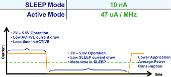
Interestingly, a number of applications involving a smarter (more intelligent) kinds of lighting solutions revolve around what the luminary does when it is NOT active. In such cases, the MCU must be alert and operating meanwhile, its power consumption becomes the dominant component of the entire application power budget. You will be pleased to learn that the PIC12HV752 has one of the lowest active power consumption numbers (if not the absolute lowest) among all embedded microcontrollers available on the market, as of this writing. This has been characterized to be below 45uA/MHz (@2V).
When the device is inactive (Sleep), i.e., not executing code and all peripherals are disabled, the core consumption drops to 10nA, a value so small it challenges the resolution of any instrumentation you might have on your desk.
#8 Volatility
The PIC12HV752 is a Flash microcontroller, which means that its program memory contents can be rewritten hundreds of thousands of times. This provides the product with a longer life span as new code can be injected even when deployed in the field. But, wait there is more. The microcontroller can use a portion of its Flash program memory to store parameters at run time. The PIC12HV752 flash memory is guaranteed for 100,000 erase/write cycles and 40 years of data retention. Granted, this is not the exact equivalent to the functionality of a proper data EEPROM, yet the PIC12HV752’s Flash memory can prove more than adequate for many lighting applications, in order to:
• Store a unique serial number (re-assignable)
• Permanently record a few set points (current, voltage, temperature…)
• Permanently record calibration values
• Perform logging
• Maintain a usage count
#9 Space
The PIC12HV752 is offered in 8-pin packages, a feat made possible by itshigh integration and the flexible internal connections offered. This includes some relatively (physically) large packages, such as DIP8 and SOIC8, which are very handy for quick prototyping and lab experimentation. Also available are minuscule packages such as the 3×3mm DFN option, which combines small dimensions with relatively large pitch (0.6mm), which means ease of use and low cost of assembly.
#10 Cost
Not only will the PIC12HV 752 be your lowest cost item on the BOM, with prices starting at 0.56 USD for a quantity of 10,000, but you should appreciate how few other components will be required to provide the complete solution. Beyond all the other elements already mentioned in the previous points, consider the fact that, on-chip, you will find already integrated:
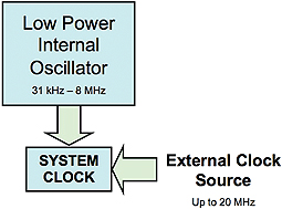
• Precision Oscillator (1% factory tuned) with selectable 8MHz, 4MHz, 1MHz and 31KHz output options
• Power-on and brownout-detect reset circuits
• Watchdog timer
• 4 Timers (3×8-bit, 1×16-bit)
• 1 Capture, Compare PWM module
• Pull up/down resistors on each I/O pin
• In-Circuit Programming and Debugging interface
Conclusions
I hope these ten short points have helped you appreciate the advantages of choosing the PIC12HV752 microcontroller to design small, cost-effective, and efficient LED drivers. Similarly, any other DC/DC conversion application (e.g., small power supplies, battery chargers…) that needs the intelligence and flexibility of a microcontroller with the ease of use of an analog switcher will benefit from the same combination of analog integration and simplicity.
References
• PIC12HV752 Datasheet: (www.microchip.com/wwwproducts/Devices.aspx?dDocName=en552818)
• High Power LED Flashlight Demonstration (http://ww1.microchip.com/downloads/en/DeviceDoc/41625A%20.pdf)
• Next-Generation Peripherals Brochure (http://ww1.microchip.com/downloads/en/DeviceDoc/41565c.pdf)
PIC is a registered trademark of Microchip Technology Incorporated in the U.S.A., and other countries.
www.microchip.com