


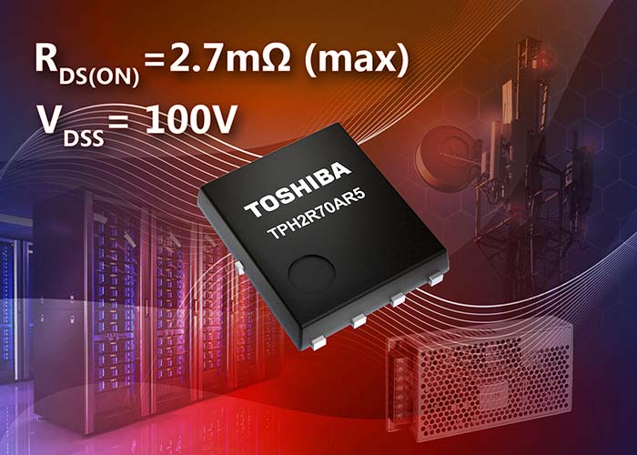
Toshiba launches 100V N-channel power MOSFET – TPH2R70AR5 – offering 2.7mΩ in 5.15mm x 6.1mm package based on U-MOS11-H process
Toshiba has launched the TPH2R70AR5, a new 100V-rated N-channel power MOSFET fabricated with its latest-generation process, known as U-MOS11-H. The MOSFET will be primarily used in switched-mode power supply (SMPS) applications, particularly high-efficiency DC-DC converters. Key application sectors will be within data centres, communications base stations, and other high-end industrial equipment.
Features
Due to the advanced 100V U-MOS11-H process, the TPH2R70AR5 offers significant performance advantages over devices manufactured with the existing U-MOSX-H process. For example, compared to the earlier TPH3R10AQM, the drain-source on-resistance (RDS(ON)) has reduced by around 8% to just 2.7mΩ (max.) while the total gate charge (Qg) is now 37% lower at 52nC (typ.). The RDS(ON) x Qg figure-of-merit (FoM) is therefore improved by 42%.
In addition, the TPH2R70AR5 achieves high-speed body diode performance through the application of lifetime control technology. As a result, compared to the TPH3R10AQM, switching speed is improved and, additionally, the diode recovery time and noise are reduced. Lifetime control technology also reduces reverse recovery charge (Qrr) to 55nC (typ.) and suppresses voltage spikes. The RDS(ON) x Qrr FoM is improved by around 43%.
The prominent RDS(ON), Qg, and Qrr characteristics reduce both conduction and switching losses, contributing to higher efficiency in power-related applications. This reduces the operating cost and permits greater power density. Housed in the SOP Advance (N) package measuring just 5.15mm x 6.1mm, the device offers excellent mounting compatibility with industry standards.
The new TPH2R70AR5 is rated for a maximum drain current (ID) of 190A at an ambient temperature of 25°C. The device is capable of operating with a channel temperature (Tch) up to 175°C, thereby reducing the need for cooling measures.
Toshiba also offers circuit design support tools: the G0 SPICE model, which verifies circuit function in a short time, and highly accurate G2 SPICE models that accurately reproduce transient characteristics. All support tools are now available via a free download from Toshiba’s website.
Shipments of the TPH2R70AR5 start with immediate effect.
Toshiba will continue to expand its lineup of low-loss MOSFETs that enable more efficient power supplies and contribute to lower equipment power consumption.
Read more about the new TPH2R70AR5 N-channel power MOSFET on Toshiba’s website: https://toshiba.semicon-storage.com/eu/semiconductor/product/mosfets/12v-300v-mosfets/detail.TPH2R70AR5.html