


The venerable Intel 8051 device is still alive and well today. The architecture has been modernized to suit today’s process technologies and computational needs. These modern 8051-based microcontroller (MCU) architectures still manage to maintain code compatibility with the original Intel devices, but to improve performance, they have long sacrificed cycle accuracy.
A multitude of architectural variations exist today including the Silicon Labs MCU version, which has evolved into a pipelined complex instruction set computing (CISC) device with Fetch/Decode/Execute pipe stages. This core is known as the CIP-51 as developed by Silicon Labs and sits at the heart of all its 8-bit mixed-signal MCUs.
Author:
Tom David, Principal Design Engineer, Microcontroller Products at Silicon Labs
Benefits of the 8051 Architecture
The 8051 architecture is well suited as a CPU for today’s small-form-factor, feature-rich MCUs. This architecture enables the easy addition of on-chip peripherals as well as flexible I/O, thus enabling an easily extensible portfolio of 8-bit devices. A few capabilities have been added to the 8051 architecture that impact backward compatibility; but backward compatibility will only be affected if these capabilities are enabled. (Figure 1 shows the CIP-51 architecture.)
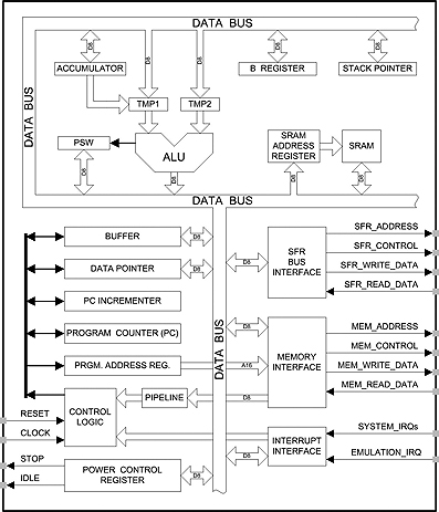
Figure 1 shows that the base architecture is almost identical to the original 8051, thus maintaining instruction-level compatibility. This controller can perform its computational function quite well even when compared with some of today’s more advanced CPU architectures. For example, most RISC machines that are register-based will only allow arithmetic logic unit (ALU) operations on values stored in the register file. Thus, to “AND” two values together, the values first have to be moved to the register file before they can be operated on.
However, in the 8051 architecture, this operation can be performed on values stored in some of these peripheral registers directly. This approach enables the controller to perform fast control functions.
If the application needed to turn around an I/O port based on the polarity of another I/O pin or pins, this task could be performed with a simple test or logical operation of the controlling I/O pin/bus and then a “write” to the relevant port control logic to turn the port around.
With the 8051 architecture, these functions can be done in two cycles, thus enabling fast control response time. This kind of speed can only be dreamed of in modern 16-bit and even 32-bit architectures with their multitude of bus hierarchies and non-deterministic event generation logic.
Another common misconception of an 8-bit controller such as the 8051 is that its code density is poor in comparison to more modern 16- and 32-bit architectures. There are of course some functions that don’t implement well on 8-bit architectures such as a 16-bit by 16-bit multiply. Operations like this do expand on an 8-bit machine. The code density for this kind of operation can be mitigated through the implementation of a 16 by 16 hardware multiplier, for example.
In general, control type applications that deal in byte-sized data do not suffer this consequence. In addition, because 8-bit machines have very little overhead code, overall code density for control type functions are lower than equivalent functions implemented on non-8-bit machines.
An additional misconception of the 8051 architecture is that interrupt servicing can be slow and the need to store and restore state can take time. The 8051 handles multiple threads via its 32-register banked register file. When an interrupt is taken and the state of the register file has to be preserved, simply switching to a different bank enables fast context switching. Of course, this approach does not preclude having to save off the accumulator and a few other relevant registers.
The original 8051 architecture only supported two interrupt priorities. This definition worked well on devices with small peripheral sets, but as peripherals sets have grown, so has the need for a finer granularity in interrupt handling.
The newer 8051 devices from Silicon Labs support up to four interrupt priorities. Having a finer interrupt granularity allows more predictable real-time functioning in a peripheral-rich environment.
Another limitation of the 8051 core (and other 8-bit architectures) is that the total code space available is limited to 64Kbytes. Some of these 8-bit devices with a rich set of peripherals will potentially use code stacks far greater than the available 64K byte address map. To accommodate this need, Silicon Labs implemented an innovative code banking technique in its 8051-based MCUS that enables expansion of this space. This technique, when coupled with a “C” compiler that comprehends the feature, makes this space look seamless to the software writer, thus imposing no burden.
The 8051 architecture natively supports only 256 Special Function Registers (SFRs). This restriction imposes quite a burden on resource-rich devices. To alleviate this limitation, Silicon Labs introduced a paging capability to the SFR map. This feature supports the use of much larger register spaces. Some of the larger 8-bit devices released by Silicon Labs use up to five pages.
Most of these devices have at least two pages where one page is dedicated to debug control logic and cannot be accessed by the developer.
In a modern fetch, decode and execute machine, there is a great dependence on having a fast memory interface. This capability enables instruction fetches on every cycle. When implemented with flash memory, this approach becomes challenging since flash access speeds generally can’t keep up with the speed of the CPU. To alleviate this situation, most 8-bit MCU vendors add instruction prefetch buffers and/or caches.
Prefetch buffers enable defined execution during straight line code execution, and when branching the only cycle penalty paid is equal to the depth of the prefetch buffer, which in most cases is just 2 bytes wide except in the case of Silicon Labs’ ultra-high-speed 100 MHz 8051-based MCUs where the buffers are four bytes wide.
A cache will create no looping penalty as long as the loop fits in the cache, but if it misses the cache, the miss penalty can inject a lot of indeterminism into the instruction stream.
Thus, real-time responses could suffer. Instead of implementing a cache, Silicon Labs has implemented branch target buffers and prefetch buffers on some of its faster 8-bit devices.
Flash or non-volatile memory (NVM) security is another issue that arises with 8-bit MCUs.
To address this issue, Silicon Labs has implemented multiple flash regions in its 8-bit MCUs that offer varying levels of protection. This technique allows MCU vendors to ship MCU products to their customers who might need to program their software IP into the MCUs while using the vendor’s software drivers and APIs.
State-of-the-Art 8051-Based MCU Example
Figure 2 shows the C8051F850 MCU from Silicon Labs, which is an example of a modern MCU that uses the CIP-51 as its core. This 8-bit device is available in industry-standard small-footprint 16-, 20- and 24-pin packages.
The integration level available in the 8-bit MCU shown in Figure 2 is second to none for its size and cost. The SAR-ADC is 10-bit/800 ks or 12bit/200 ks capable. The mixed-signal peripheral integration with this degree of performance is not found anywhere else in the MCU market at this size and cost.
This functionality is enabled because the high-speed CIP-51 core can support the throughput of these peripherals.
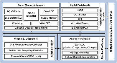
Also note that since this is a peripheral-rich but pin-limited device, Silicon Labs implemented a priority crossbar encoder that allows any peripheral to access any pin.
This crossbar architecture provides flexibility and ease of use and allows simpler PCB implementations.
The heart of any system-on-chip (SoC) device is its CPU. If the CPU is inadequate, then the entire SoC performance suffers. Thus, building a compelling SoC with an abundance of high-performance peripherals requires using a CPU capable of operating on all the data generated by these peripherals. This level of performance is not commonly found in the 8-bit market. However, this is where the CIP-51 architecture outshines all other 8-bit cores.
Since this CIP-51 core is still 8051 instruction compliant, the ecosystem for development tools, software and drivers is very rich and diverse, thus driving down development cost while keeping the quality of the embedded design relatively high.
Conclusion
In today’s ARM-oriented MCU development environment, 8-bit devices might look old and a bit long in the tooth, but looks are deceiving. When coupled with modern process technologies and advanced mixed-signal peripherals, 8-bit performance on most control tasks can match or exceed many other CPU architectures.
Coupled with modern, more capable peripherals, these 8-bit machines can offer a cost-effective solution that might preclude the need to move to a higher bus-width device, thus saving development time and money.
www.silabs.com