


 Objective
The objective of this lab activity is to investigate simple transresistance amplifier input stage configurations.
Background
A transresistance amplifier outputs a voltage proportional to its input current. The transresistance amplifier is often referred to as a transimpedance amplifier, especially by semiconductor manufacturers. The general description for a transresistance amplifier in network analysis is a current controlled voltage source (CCVS).
An inverting transresistance amplifier can be configured from a conventional operational amplifier and a single resistor. The resistor is connected between the output and the inverting input of the operational amplifier and the noninverting input is connected to ground. The output voltage will then be proportional to the input current at the inverting input node, decreasing with increasing input current and vice versa.
The activity in this lab exercise investigates an alternate differential input structure that produces an inherently low input impedance (a current input) as opposed to the relatively high input impedance of the voltage differential pair that was investigated in the June StudentZone activity and July StudentZone activity (MOS). A complete transresistance amplifier may require the addition of more gain stages and an output driver stage.
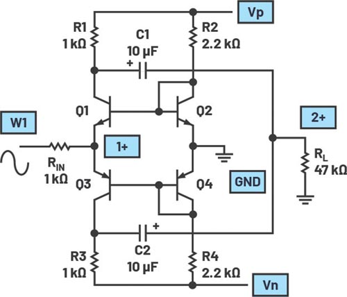
Figure 1. A transresistance amplifier input stage with current drive.
Materials
- ADALM2000 Active Learning Module
- Solderless breadboard
- Jumper wires
- Three 1 kΩ resistors
- Two 2.2 kΩ resistors
- One 47 kΩ resistor
- Two 10 μF capacitors
- Two NPN transistors (2N3904 or SSM2212)
- Two PNP transistors (2N3906 or SSM2220)
Directions
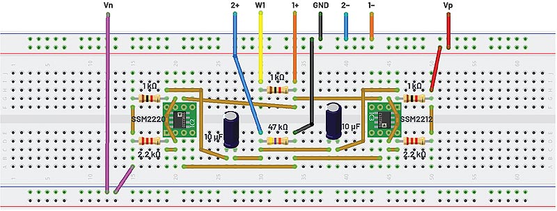
Figure 2. A transresistance amplifier input stage with current drive on a breadboard circuit.
The circuit and the connections to the ADALM2000 are shown in Figure 1. NPN transistors Q1 and Q2, as well as PNP transistors Q3 and Q4, should be selected from the available devices with the best matching VBE. Transistors fabricated in the same package, such as the SSM2212, SM2220, or the CA3046, tend to match much better than individual devices. Scope Input 1+ may optionally be connected to the junction of the Q1 and Q3 emitters or the collectors of either Q1 or Q3 while investigating the operation of this circuit. The current input node at the junction of the emitters of Q1 and Q3 is nominally low impedance so it can be driven from a current source. The AWG outputs of ADALM2000 are more like voltage sources. Thus, the 1 kΩ resistor RIN serves to convert the voltage output of AWG1 to a current (IIN = VIN/1 kΩ).
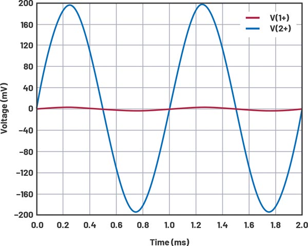
Figure 3. The waveforms of a transresistance amplifier input stage with current drive.
Hardware Setup
The first waveform generator, W1, should be configured for a 1 kHz sine wave with 800 mV peak-to-peak amplitude and 0 offset. Channel 1 of the scope should be connected to display the output of the first generator and Channel 2 should be set to display the output signal at 40 mV per division.
Procedure
Configure the oscilloscope to capture several periods of the two signals being measured. A plot example using LTspice® is presented in Figure 3.
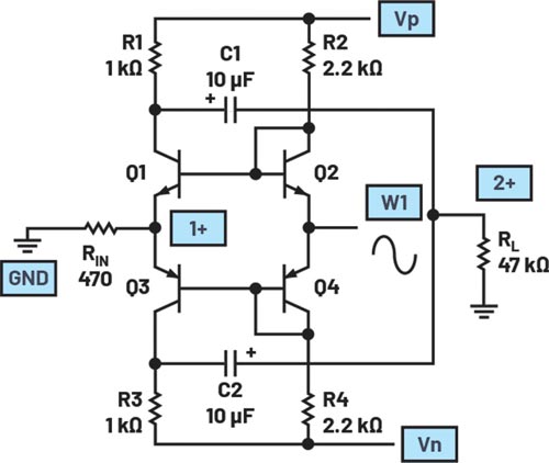
Figure 4. Differential pair with tail current source.
Observe the output at RL, which is the AC-coupled sum of the signals at the collectors of Q1 and Q3. Measure the voltage gain from the AWG1 output to RL and compare it to your calculated value. Observe the voltage amplitude of the signal seen at the at the current input node (1+), where the emitters of Q1 and Q3 are connected. Based on the amplitude, calculate the input current amplitude (the voltage across RIN divided by RIN) and the effective input resistance of the amplifier. Compare these values to your calculated values.
Configure for Voltage Drive
Additional Materials
- One 470 Ω resistor
Directions
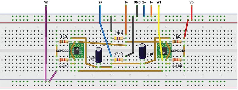
Figure 5. A transresistance amplifier input stage with voltage drive on a breadboard circuit.
Now we are going to reconfigure the input for voltage drive. Replace RIN with a 470 Ω resistor and ground the other end, as shown in Figure 4. Disconnect the emitters of Q2 and Q4 from ground and connect them to the output of AWG1.
Hardware Setup
The first waveform generator, W1, should be configured for a 1 kHz sine wave with 800 mV peak-to-peak amplitude and 0 offset. Channel 1 of the scope should be connected to display the output of the first generator and Channel 2 should be set to display the output signal at 80 mV per division.
Procedure
Configure the oscilloscope to capture several periods of the two signals being measured. A plot example using LTspice is presented in Figure 6.
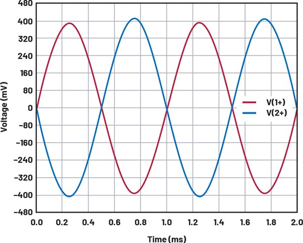
Figure 6. The waveforms of a transresistance amplifier input stage with voltage drive.
Observe the output at RL, which is the AC-coupled sum of the signals at the collectors of Q1 and Q3. Measure the voltage gain from the AWG1 output to RL and compare it to your calculated value. Observe the voltage amplitude of the signal seen at the current input node (1+), where the emitters of Q1 and Q3 are connected. Based on the amplitude, calculate the input current amplitude (the voltage across RIN divided by RIN) and the effective input resistance of the amplifier. Compare these values to your calculated values.
To measure the current that is required from the input driver (W1) in this voltage drive configuration, insert the 1 kΩ resistor in series with AWG1 (and the emitters of Q2 and Q4). Connect the differential Channel 1 scope inputs 1+, 1– across the 1 kΩ resistor. Observe this voltage and calculate the current as AWG1 swings over the ±400 mV swing.
Questions:
- Name the main characteristic that defines a transresistance amplifier.
- Can you identify applications that use this type of circuit? You can find the answers at the StudentZone
About the Authors
 Doug Mercer received his B.S.E.E. degree from Rensselaer Polytechnic Institute (RPI) in 1977. Since joining Analog Devices in 1977, he has contributed directly or indirectly to more than 30 data converter products and he holds 13 patents. He was appointed to the position of ADI Fellow in 1995. In 2009, he transitioned from full-time work and has continued consulting at ADI as a Fellow Emeritus contributing to the Active Learning Program. In 2016 he was named Engineer in Residence within the ECSE department at RPI. He can be reached at doug.mercer@analog.com.
 Antoniu Miclaus is a system applications engineer at Analog Devices, where he works on ADI academic programs, as well as embedded software for Circuits from the Lab®, QA automation, and process management. He started working at Analog Devices in February 2017 in Cluj-Napoca, Romania. He is currently an M.Sc. student in the software engineering master’s program at Babes-Bolyai University and he has a B.Eng. in electronics and telecommunications from Technical University of Cluj-Napoca. He can be reached at antoniu.miclaus@analog.com.
![]()
Visit: https://ez.analog.com
Contact Romania:
Email: inforomania@arroweurope.com
Mobil: +40 731 016 104
Arrow Electronics | https://www.arrow.com
![]()