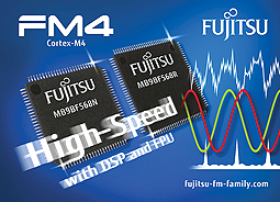
In addition to Fujitsu’s FM3 microcontroller (MCU) family, MSC will offer Fujitsu’s new FM4 family of MCUs, which are based on the ARM® Cortex™-M4F processor core. The new FM4 family consists of a total of 84 MCUs and is suited for applications where the main requirement is high processing power.
The M4F RISC processor core, which incorporates digital signal processor (DSP) and floating point unit (FPU) functions, is designed for high clock frequencies of up to 160 MHz. Thanks to a low current consumption of approximately 1.5 µA in real-time mode, these high-performance MCUs can even be operated in standby mode operation with battery buffering.
The FM4 MCUs also offer a range of memory options to ensure high-performance and energy efficiency. The MCUs, which are equipped with an external bus connection for SRAM, SDRAM, NAND flash and NOR flash, have a 128-bit ultra-wide bus for on-chip flash memory that enables read access with no CPU wait state. The up to 1.5 MB flash memory is specified for a total of 100,000 write/read cycles and data retention of up to 20 years. Furthermore, in order to enable a high level of functional safety and facilitate certification, a range of hardware functions — such as error correction code (ECC) flash, cyclic redundancy check (CRC) and memory protection unit (MPU) — were implemented on the FM4 MCUs.
The new FM4 family of MCUs builds on Fujitsu’s FM3 MCU family, and offers even more performance and peripheral functionality. For example, new trimming functions deliver internal oscillator accuracy of ±2 percent and the 12-bit A/D converter operates at twice the speed of previous versions.
The multifunction timer for three-phase motors also features a number of enhanced functions, such as support for asymmetric PWM waveform output and multiple A/D start triggers. The minimum timing resolution possible is 6.25 nanoseconds. Furthermore, a Descriptor System data Transfer Controller (DSTC) was implemented to reduce the CPU’s workload and software overhead. The redesigned communications IP and clock rates of up to 20 MHz improve high-speed serial data communications via the serial peripheral interface (SPI).
MSC Vertriebs
www.msc-ge.com


