


In many systems microcontrollers are used to control multiple Point-Of-Load (POL) DC/DC converters forming a hybrid control system to manage system start-up behavior, monitor electrical parameters and manage the power consumption of peripheral sub-systems. The most sophisticated solutions, however, can be found on motherboards of computers, graphic cards or on CPU blades of servers, where Voltage Regulator Modules (VRM) directly communicate with their load to adjust supply voltages and/or even adapt their control characteristic to temporary operation conditions. This kind of “intelligent” power conversion management and control offers significant advantages in terms of total system efficiency, performance and reliability – in short: preferences which are dominant in industrial, medical, automotive and consumer market segments as well.
by Andy Reiter, Microchip Technology Inc.
Since almost one decade Microchip Technology Inc. focuses on so-called intelligent resp. smart power conversion (IPC/SPC) applications to bring more features and enhanced capabilities to all sorts of power conversion applications. One main focus has been, and still is, the fully digital control of power converters/inverters using DSP-based, high performance microcontrollers with highly dedicated high-speed, high resolution peripherals as well as dedicated controller families for hybrid control systems combining microcontrollers with fully analog based control loops. Looking into the particular solutions more closely, it becomes obvious, that neither the analog-based hybrids nor the fully digital solutions are 100% analog or 100% digital. Both urgently need their analog and digital counterpart to overcome certain limitations and therefore offer specific strength for their specific target applications. The latest product family of smart power conversion controllers MCP191xx marks a new technological step in making power converters more intelligent and focuses on dedicated power converter topologies and applications.
The first members of this family of products MCP19111 are merging an analog high-performance synchronous buck converter controller and an 8-bit MCU into one monolithic IC, offering enhanced, flexible configuration, control and monitoring capabilities as well as they allow the integration of standardized or proprietary communication to align multiple converters within a higher power management structure. In contrast to other existing hybrid POL controllers, the MCP19111 are fully programmable in C-language. This advantage offers full flexibility to adjust the device to many different application requirements, to adapt to certain operating conditions, to implement generic monitoring tasks and customized features. The wide input voltage range of 4.5V to 32V DC and output voltages as low as 0.5V together with drivers supporting up to 2A source/4A sink opens a wide variety of applications to be supported.
Digital Enhancements
Having a digital controller on the same die as the analog switching regulator makes it possible to dovetail analog functions and digital control very tightly enabling direct manipulation of the compensation circuit, switching frequency, dead-time control, system level thresholds and many other features during runtime.
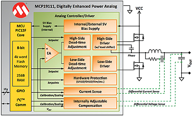
Furthermore, as the MCU itself is encapsulated in the analog switching regulator architecture, the need for additional auxiliary power supplies or external MOSFET drivers has been eliminated. Figure 1 shows a high-level block diagram of the MCP19111 Digitally Enhanced Power Analog Controller together with a typical application circuit. The analog switching regulator section fully covers all components of the analog control loop including the MOSFET drivers and also contains the auxiliary supply for the MCU. The digital section consists of an 8-bit PIC12F mid-range MCU core with 8 kB of Flash and 256 byte of RAM. It further offers up to 15 GPIOs, of which eight are additional analog inputs, an I²C/SMbus based serial communication interface, external interrupts and three free timers. Many internal signals like the input voltage, output voltage or the inductor current can be monitored directly on-chip without need for external sensing. The digital implementation even allows reading the current duty ratio, a very useful feature which was, up to now and for many technical reasons, reserved to fully digital controllers only.
Maximizing Efficiency
Besides the enhanced monitoring capabilities the monolithic integration of a digital core also gives direct access to many parameters, which are typically fixed in hardware or inaccessible in silicon. The most remarkable ones are the adjustable dead-time, the programmable compensators, internal feedback calibration, programmable protection thresholds and even the capability to switch over between current and voltage mode control during runtime.
Adjustable Dead-Bands
In synchronous buck converters the dead-time setting between high- and low-side switch has significant influence on the total efficiency of the system.
If analog controllers offer any adjustable dead-time settings at all, the designer has to refer to some sort of worst case scenario considering the highest temperatures and load conditions, where the dead-time typically needs to be at maximum, and “program” this value in hardware e.g. by placing capacitors and/or resistors. This inevitably results in increased core and diode losses as the converter will most probably be never exposed to these assumed worst case conditions.
One proper solution would be to automatically adapt the dead-time to certain load and temperature conditions. Unfortunately using an on-board zero-crossing detector to always drive the switches with an optimum dead-time has certain serious limitations for two reasons. First, all kinds of analog zero crossing detectors are based on comparators. The fastest (affordable) analog comparators have typical propagation delays of 15-20ns, which is, given the results shown in figure 3, too slow to reach the optimum level. Second, this zero-crossing detector would have to operate in the switching node of the half-bridge where the high frequency switching noise would require filters, which would slow down the trigger even more, eventually making this feature effectless.
However, where the analog domain fails, the digital domain offers a solution. The most common technique used to accomplish this optimization is to monitor and analyze the converter’s outer conditions until they become stable. As soon as a steady state operation is detected, the dead-time is modified and the duty ratio of the high-side switch is monitored.
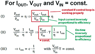
The theory of this technique for constant voltage converters is that under steady state conditions, the shortest relative on-time of the high-side switch determines the point of highest efficiency, as in this point the least amount of power has to be drawn from the bus to provide a certain, constant output power (see Figure 2).
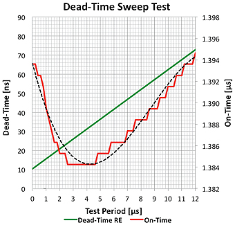
Figure 3 shows results of one single sweep over a defined range of dead-time settings during steady state operation, measured on a test bench. The green line shows the dead-time applied to the rising edge of the high-side switch (DTR). The red curve gives the development of the on-time of the high-side switch over the different dead-time settings, the dotted black line shows its 3rd order approximation.
The given range for the dead-time sweep was determined by characterizing the system and defining a best-case scenario (shortest dead-time) and a worst-case scenario (longest dead-time). The sweep was performed with the maximum resolution of 4ns at 90% load (Vin = 12V, Vout = 3.3V, Iout = 9A). On the left side of the chart, the duty-cycle starts with values of around 1.394 µsec and rapidly drops as soon as the dead-time is increased. In this area the high- and low-side switch already show some overlap and some of the power drawn from the input is directly shorted to ground.
At dead-times around 25ns the on-time reaches its minimum of 1.384 µsec and starts to rise again when the dead-time is further increased. In a non-adjustable design, the dead-time would have been adjusted to at least 70ns for the switches used, so the typical on-time for this operating condition would have been 1.395 µsec. In accordance with equation III of figure 2, the difference between the original and optimized high-side on-time is 11ns wide. On the first glimpse this doesn’t sound much, but in this high frequency converter it stands for ~0.9% increase in efficiency resp. an in increase in total efficiency from ~92% to 93%.
Adjustable Switching Frequency and Compensation Network
One additional very nice feature is the capability to adjust the compensation network and switching frequency by software. This not only eases the basic adjustment during setup configuration, it also allows to make adjustments during runtime. This, so far, has been the unreachable core domain of fully digital controllers. In hard-switching topologies like synchronous buck converters, the switching losses are dominantly responsible for the majority of power losses. To
improve the efficiency especially at light loads, reduction of the switching frequency can significantly help to improve the total efficiency of the converter. However, when the switching frequency is being reduced while the compensation network is fixed in hardware, commonly the gains start to drop and might result in a loss of phase and gain margin. To compensate this effect, an adjustment of the system’s gains is required.
The MCP19111 offers registers to adjust the ramp voltage of the PWM generator, the zero frequency (resonance frequency at the origin, defining the first pole), the total gain and slope gain as well as the slope itself. Further there are register sets to adjust the amplifier offset and current sense gain. Although this technique might require a process of extensive system characterization, it bares the chance for significant improvements in terms of efficiency and stability.
Very Light Load Efficiency Optimization
In asynchronous buck converters the power losses in the freewheeling diode are determined by the forward voltage drop times the current. As the significant forward voltage drop across the diode is present permanently and cannot be minimized, an additional switch with significantly lower forward voltage drops is commonly used to bypass/replace the diode eventually forming a synchronous rectifier. This technique is commonly used when load currents above 1A are required. However, during light load conditions, when there is very little current flowing through the low-side switch, the power required to drive its gate exceeds the savings gained by bypassing the freewheeling diode with a switch. To support further efficiency enhancements under this particular conditions, the MCP19111 offers the so-called diode-emulation mode, where, when enabled, the low-side driver is turned off. With a disabled driver, the gate is not biased anymore and the MOSFET’s body diode will become the rectifier, minimizing the power losses.
This kind of measure to minimize partial power losses and increase the total overall efficiency can additionally be backed-up by using Microchip’s new family of power MOSFETs MCP870xx. This family of low RDS(on), well balanced Figure-Of-Merit (FOM) fast Power-MOSFETs offer a range of different On-Resistance vs. Total Gate Charge (QT) combinations to optimize the total FOM of the half-bridge. The higher QT of the low side switch, the more effective becomes the diode emulation mode of the MCP19111.
Optimizing No-Load Operation
The MCP19111 are current mode controllers to offer best performance during normal operation. However, a current mode controller needs to have at least some current flowing to function properly. When load switch into low-power standby operation, the output of the converter still has to provide the nominal output voltage, but the output power might almost be zero. Commonly current mode controllers switch into some sort of hick-up or Pulse-Frequency-Mode (PFM) operation with higher output ripples, violating line regulation tolerances and often also causing serious EMI issues. To overcome this limitation of typical current mode controllers, the MCP19111 can be switched into pseudo voltage mode control by disabling the current loop resulting in a improvement of the output voltage and system stability.
Usability and Tool Chain
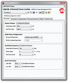
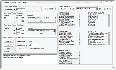
The impressive list of enhanced features of the MCP19111 offers an overwhelming number of options to configure and optimize the system. The open programmability of the MCU adds even more degrees of freedom. Therefore Microchip offers the Graphical User Interface (GUI) shown in Figure 4, which can be used to make certain adjustments and configurations without the need to write code. This GUI works with an open-source firmware, which can be modified and be used as a template to develop individual, more advanced features. In addition to the configuration interface, Microchip offers a second GUI for test purposes, enabling the user to directly communicate with the device using the PMbus protocol (see Figure 5). This GUI is working with Microchip’s PICkit Serial Analyzer (Part-Number DV164122), which is a generic low-cost USB-to-UART/SPI/I²C interface and can be directly used to monitor and debug the device during operation.
Resume
Although most of the techniques are known and some features can also be found on already existing parts, the MCP19111 family of devices opens a new chapter in the history of intelligent switching regulators. The density of dedicated features together with the free programmability makes the powerful difference. In the world of smart power controllers, the MCP19111 brings analog and digital control schemes closer together and removes existing limitations by making all features available and accessible to engineer and therefore forms the base of innovative, efficient and reliable high performance POL converters.
Author Information

Andreas Reiter
Technical Business Development Manager for Power Electronics, Europe at Microchip Technology
Short Biography:
Andreas Reiter, born in 1973, studied medical engineering and physics at the University of Applied Sciences in Munich. From 2000 he worked as developing engineer and later as director of R&D in the automation industry, before he focused on power electronics applications as senior applications engineer in 2007. Since 2010 he is responsible for application-oriented R&D of fully digital control methods and solutions in power electronics applications at Microchip Technology Inc.
www.microchip.com