


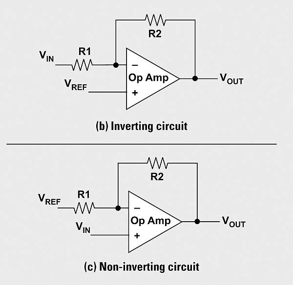
Figure 1: WEBENCH® Amplifier Designer operational amplifier design circuits.
Requirements: Mapping from many to one
The ultimate task is to find the perfect op amp for an amplifier circuit. In the case of selecting amplifiers from Texas Instruments, this challenge requires the designer to sort through approximately 1300+ op amps. These amplifiers come with many variations on their electrical perfor¬mance and specifications. The key specifications include power-supply ranges, bandwidth, input/output swing limits, and others. On top of these hard constraints, most amplifier choices use a series of overlapping issues, such as accuracy, noise, power, temperature drift, and/or IC cost.
Starting from ground zero, the first task is to sort amplifiers according to basic suitability for the final design. As step one, the designer identifies the basic-circuit operational values. These values can be entered using a web-based amplifier design tool, such as the WEBENCH® Amplifier Designer (Figure 2).
On the Amplifier Designer Requirements page (Figure 2), fields that must be completed are:
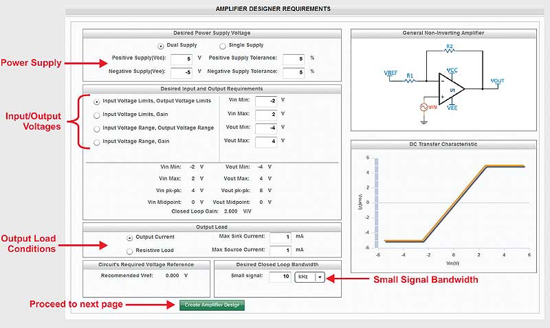
Figure 2: Amplifier Designer Requirements page for user’s data-entry activities.
• Power supply voltages
• Circuit input and output signals
• Output load conditions
• Small-signal output bandwidth
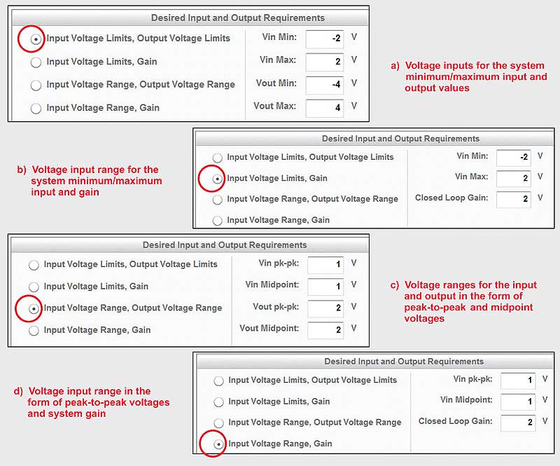
Figure 3: Voltage input and voltage output styles.
These design requirements allow the Amplifier Designer software to select an appropriate op amp for the amplifier circuit.
As a start, the provided power supply voltages can eliminate devices with supply voltages that are out-of-range. For example, the input values in Figure 2 may be for a dual-supply, ±5 V. From this infor¬mation, the software eliminates op amps with maximum power-supply ranges below 10 V, and minimum power-supply ranges greater than 10 V. Additionally, the amplifier selection process removes amplifiers with excessively-high power-supply ranges.
As for the amplifier’s input stage, the design tool ensures there is no violation to the op amp’s common-mode range. With the output stage, the software makes sure that signals remain within the rail limits of the power supply, while taking a further step to ensure that the output swing is within the candidate-amplifier’s linear region. To achieve this, the software uses the amplifier’s output load conditions.
The tool offers four data entry styles for input voltages, output voltages, and gain. It also accommodates individual designer preferences as shown in Figure 3.
For the last data entry, the design tool uses the small-signal bandwidth to identify suitable amplifiers. In an effort to take the amplifier’s process variations into account, the applied guard band for this specification is approximately 20 percent.
These data inputs were used for the discussion on the following pages:
VCC = 12 V
VEE = 0 V
VINMin = 5.5 V
VINMax = 6.5 V
VOUTMin = 0.5 V
VOUTMax = 11.5 V
IOUT source/sink current = 1 mA
Small signal bandwidth = 500 kHz
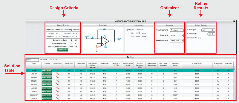
Figure 4: Amplifier Designer Visualizer screen.
Screening op amps to target: Visualizer screen
![]() The next design screen was obtained by clicking the Create Amplifier Design button. During the transition from the view in Figure 2 to Figure 4, the software determines the resistor values in the target op amp circuit. It is easy to assign a generic feedback resistor (R2) value of 1 kΩ. However, a better general guide is to assign the values according to Table 1.
The next design screen was obtained by clicking the Create Amplifier Design button. During the transition from the view in Figure 2 to Figure 4, the software determines the resistor values in the target op amp circuit. It is easy to assign a generic feedback resistor (R2) value of 1 kΩ. However, a better general guide is to assign the values according to Table 1.
The algorithms that produce the Amplifier Designer Visualizer screen shown in Figure 4 create a reduced list of op amps. The order of the amplifiers listed depends on which optimizer parameters have been selected.
On the top left of Figure 4 is a list of input Design Criteria and to the right is the Optimizer box.
The Optimizer box has three pull-down menus with the following options to set design priorities:
• Precision • Noise • Temp Drift • Supply Current • Cost
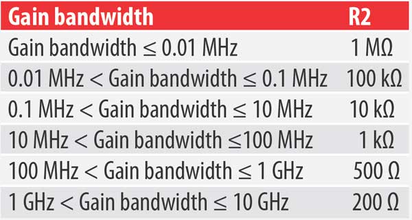
Appropriate voltage-feedback amplifier (VFB) R2 resistance values.
The question to ask is, of these five characteristics in the Optimizer pull-down menus, which is the Very Important, Important, and Less Important? When the choice is completed, the Solution Table in Figures 4 shows updated results.
Additionally, further criteria refinements are possible with the menu in the upper right corner of Figure 4. The choices available in this area are:
• Package Group
• Number of Channels
• Shutdown Pin
The selections in this section are self-explanatory, however, these selections further reduce the list of amplifiers.
When the Optimizer menu options are changed such that Precision is selected as Very Important, Temp Drift as Important, and Supply Current as Less Important, the OPA140 should appear near the top of the list in the Solution Table.
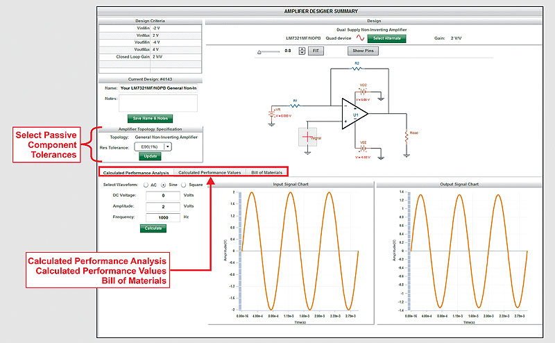
Figure 5: Amplifier Designer Summary screen.
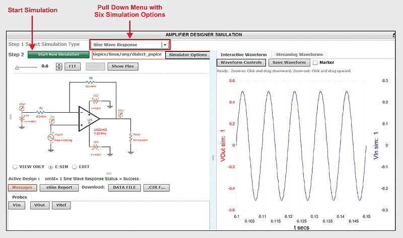
Figure 6: Amplifier Designer Simulation screen.
![]() Designer summary screen
Designer summary screen
The next step is to proceed on to the Amplifier Design Summary screen. For the following discussion, the Open Design button was selected for the OPA140 in the Solution Table of the Visualizer screen. At this point, the amplifier has been selected and the circuit fully defined. The Amplifier Designer Summary screen (Figure 5) allows exploring the theoretical feasibility of the design. The center bar in Figure 5 shows selection tabs for viewing Calculated Performance Analysis, Calculated Performance Values, and the Bill of Materials. The Calculated Performance Analysis segment produces input/output graphs as shown in Figure 5. There are menu selections to view AC, sine and square-wave graphical responses. These curves are not a result of a simulation; rather the page shows calculated theoretical graphs. The intent is to provide a quick look at the circuit’s behavior before proceeding any further. The Calculated Performance Values tab allows viewing circuit characteristics in seven categories:
1. Design criteria
2. Operating frequency values
3. Power requirements
4. VOS/Ib error
5. VOUT gain versus resistor tolerance
6. Error over temperature
7. Total output noise
Within these seven categories, there are calculated performance values. For instance, the operating frequency values (#2 above) provides the amplifier bandwidth, amplifier slew rate, closed-loop bandwidth, and full-power bandwidth (FPBW).

Sim
Amplifier designer simulation
To proceed to the TI SPICE simulation screen, click on the Sim button at the top of the screen (not shown in Figure 5). The Amplifier Designer ports the complete circuit to the simulation screen. The Amplifier Simulation environment (Figure 6) uses Texas Instruments PSPICE® models while providing six simulation options:
1. Sine wave
2. Step response
3. Closed loop response
4. DC sweep
5. Total noise
6. Group delay

Sim Export
With all of these simulation options, the Amplifier Designer provides the appropriate signal sources. There are options to modify the magnitudes, frequency, and timing of these sources.
If this simulation environment is not suitable, it is possi¬ble to download the circuit into a TINA-TI™ environment. WEBENCH® Amplifier Designer offers this export option by clicking on the Sim Export button at the top of the simulation screen (not shown in Figure 6).
Conclusion
The WEBENCH Amplifier Designer tool automatically performs the basic analysis and product-selection activi-ties that designers would normally perform in their circuit design activities – but it takes the process a step further. It offers a comprehensive evaluation of the new circuit, making it easy to fit the amplifier design into the rest of the system design.
Related Web sites
Design tools:
WEBENCH® Amplifier Designer
TINA-TI™ SPICE-Based Analog
Simulation Program
Product information: OPA140
Subscribe to the AAJ: www.ti.com/subscribe-aaj
By Bonnie C. Baker
WEBENCH® Senior Applications Engineer
Texas Instruments | www.ti.com