


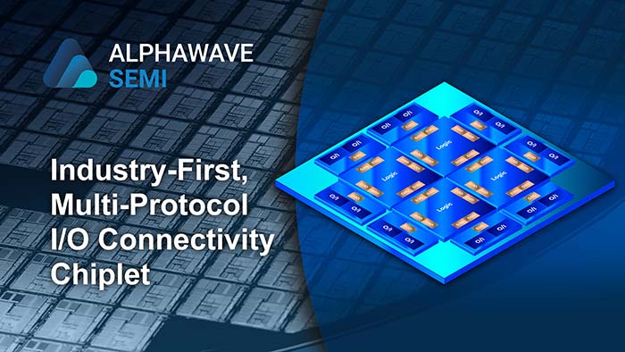
 Alphawave Semi a global leader in high-speed connectivity and compute silicon for the world’s technology infrastructure, today announced the successful tape-out of the industry’s first off-the-shelf multi-protocol I/O connectivity chiplet on TSMC’s 7nm process. Aggregating the company’s flexible and customizable connectivity IP, custom silicon and advanced packaging capabilities, the 7nm multi-standard I/O chiplet delivers a standards-compliant IP portfolio of Ethernet, PCIe®, CXL® and UCIe™ (Universal Chiplet Interconnect Express) Revision 1.1 product.
Chiplets are becoming increasingly important in high-performance compute (HPC) and artificial intelligence (AI) applications as they provide essential connectivity at a higher bandwidth and lower power than traditional infrastructure technologies without the need for extensive customization or development. By choosing commercial off-the-shelf chiplets, end customers can optimize performance and efficiency while benefiting from reduced development time, lower costs, and greater flexibility with their existing hardware ecosystems.
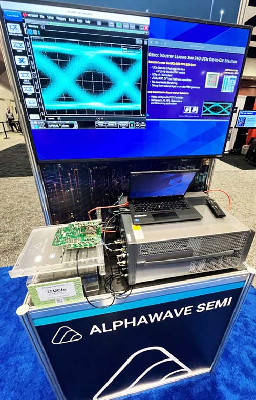
Alphawave Semi 24Gbps UCIe silicon platform
Delivering a total bandwidth of up to 1.6 Tbps, the Alphawave Semi chiplet enables up to 16 lanes of multi-standard PHY supporting silicon-proven PCIe 6.0, CXL 3.x, and 800G Ethernet in a combination of mixed operating modes. The announcement of the successful tape-out also paves the way for a robust, open chiplet ecosystem that accelerates connectivity for high-performance AI systems by employing UCIe as a die-to-die connectivity subsystem. An industry-first live demo of Alphawave Semi’s 24 Gbps UCIe silicon platform was recently unveiled at the Chiplet Summit 2024 in Santa Clara, CA.
“The successful tape-out of this off-the-shelf, multi-protocol I/O connectivity chiplet demonstrates our extensive experience of using the TSMC 3DFabricTM ecosystem to integrate advanced interfaces and marks another step forward in Alphawave Semi’s mission to deliver ultra-high-performance connectivity for the critical data communications that underpin the world’s digital infrastructure,” said Mohit Gupta, Alphawave Semi’s SVP and GM, Custom Silicon and IP. “Our top hyperscaler and datacenter infrastructure customers can quickly and easily mix and match high-performance custom SoCs with our I/O connectivity or memory expansion chiplets, providing a new level of flexibility and scalability for their AI-enabled systems.”
Percy Chang, Director of Emerging Business Development at TSMC, adds “The tape-out of the Alphawave Semi multi-protocol I/O connectivity chiplet built on our 7nm process is another example of how TSMC is playing a critical role in the semiconductor platforms essential to new and emerging high-performance, high-throughput applications. We will continue to work with our VCA partners like Alphawave Semi to foster a robust and open chiplet ecosystem that delivers the high-bandwidth connectivity and compute silicon needed for HPC and AI applications.”
For more information, visit http://awavesemi.com.