
Siemens streamlines design and analysis of complex, heterogeneously integrated 3D ICs
Siemens Digital Industries Software introduced two new solutions to its Electronic Design Automation (EDA) portfolio that help semiconductor design teams address and overcome the complexity challenges associated with the design and manufacture of 2.5D and 3D Integrated Circuit (IC) designs.
Siemens’ new Innovator3D IC™ solution suite enables IC designers to efficiently author, simulate and manage heterogeneously integrated 2.5D/3D IC designs. In addition, Siemens’ new Calibre 3DStress software leverages advanced thermo-mechanical analysis to identify the electrical impact of stress at the transistor level. Together, these solutions dramatically reduce risk and enhance the design, yield and reliability of complex, next generation 2.5D/3D IC designs.
Comments
“By delivering a stress-aware multiphysics analysis solution powered by Calibre 3DStress and driven by the Innovator3D IC solution suite, Siemens enables customers to overcome the complexities and risks associated with 3D IC designs,” said Mike Ellow, CEO, Siemens EDA, Siemens Digital Industries Software. “These capabilities are critical for our customers, allowing them to accelerate productivity and meet stringent design timelines by effectively eliminating the barriers of design complexity that traditionally impact design cycles.”
Innovator3D IC solution suite
Siemens’ new Innovator3D IC solution suite delivers a fast, predictable path for planning and heterogeneous integration, substrate/interposer implementation, interface protocol analysis compliance and data management of designs and design data IP.
Built on an AI-infused user experience offering extensive multithreading and multicore capabilities to achieve optimal capacity and performance on 5+ million pin designs, the new Innovator3D IC solution suite is comprised of the Innovator3D IC Integrator, a consolidated cockpit for constructing a digital twin using a unified data model for design planning, prototyping and predictive analysis; the Innovator3D IC Layout solution for correct-by-construction package interposer and substrate implementation; the Innovator3D IC Protocol Analyzer for chiplet-to-chiplet and die-to-die interface compliance analysis; and the Innovator3D IC Data Management solution, for the work-in-progress management of designs and design data IP.
Calibre 3DStress
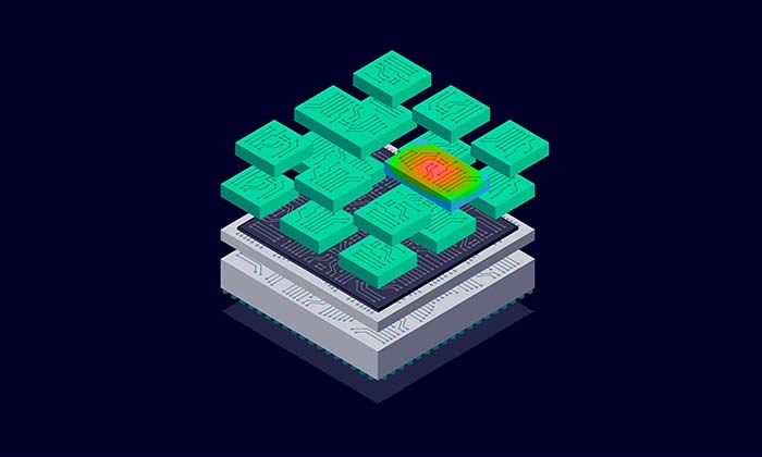
With the thinner dies and higher package processing temperatures of 2.5D/3D IC architectures, IC designers have discovered that designs validated and tested at the die level often no longer conform to specifications after packaging reflows.
Engineered to address this challenge, Calibre 3DStress supports accurate, transistor-level analysis, verification, and debugging of thermo-mechanical stresses and warpage in the context of 3D IC packaging, allowing chip designers to evaluate how chip-package interaction will affect the functionality of their designs earlier in the development cycle. This foresight not only prevents future failures but also optimizes the design for better performance and durability.
Building on the launch of Calibre 3DThermal in 2024, Calibre 3DStress expands the Multiphysics solution, dramatically reducing thermo-mechanical impacts, and delivering design and electrical behavior visibility earlier in the design process. Unlike package-level stress analysis tools, Calibre 3DStress uniquely detects transistor level stress to verify that neither packaging processes nor product functionalities will compromise circuit level performance.
Calibre 3DStress represents an important part of Siemens’ 3D IC multi-physics software portfolio and a foundational part of Siemens’ IC digital twin and semiconductor development workflows. It delivers an innovative combination of industry-standard Calibre physical verification functionality with a native and highly advanced mechanical solver to evaluate stresses in IC structures and materials.
Customer experiences with Siemens’ technologies for 3D IC design
“In 2023, we adopted Siemens’ technology to meet the complex design and integration challenges of our advanced platform solutions. The Innovator3D IC solution suite plays a critical role in enabling the high-performance solutions we deliver to AI and HPC datacenters,” said Bryan Black, CEO of Chipletz, a leading fabless AI platform provider.
“Siemens EDA’s Calibre 3DStress tool can synthesize the complexity of components, materials and processes related to 3D IC architectures and can create accurate IP-level stress analysis. Using it, ST has been able to implement early design planning and sign-off flows, and accurately model potential electrical failures due to IP-level stress within a 3D IC package. The result is improved reliability and quality, together with a reduced time to market, which provide a win both for ST and our customers,” said Sandro Dalle Feste, APMS Central R&D Senior Director, STMicroelectronics
To learn more about Siemens’ broad portfolio of solutions for 2.5D/3D IC architectures, visit https://eda.sw.siemens.com/en-US/ic-packaging/3d-ic-design/