


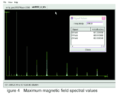
The maximum field value over the board, at each frequency step, is displayed (Figure 4). With this information, particular frequencies of interest are selected. Typically, one would select those spectral values of large amplitude. However, it should be recognized that the spectrum envelope would be modified somewhat by the proximity of other boards, the enclosure, and the cabling. A certain degree of insight is required. For example, a power cable extending from a metallic enclosure will act as an approximate quarter-wavelength monopole. It will be excited by the appropriate frequency. The spectral value, at this frequency, could be considerably smaller than the maximum value displayed on the plot resulting from the near-field simulation. Similarly, enclosure cavity resonances and aperture dimensions could enhance smaller harmonics. A fuller simulation awaits the availability of system EMC simulators that include enclosures and cables excited by emissions coming from contained printed circuit boards. Nonetheless, knowledge of frequencies of concern (specified by standards or by tests on prototypes)allows the identification of nets that are the source of the problems. Specifically, the field map at each frequency of interest (e. g. Figure 5) provides the next step in locating nets responsible for regions of high radiation. Nets that are near the “hot “regions are inspected for electrical current value at the frequency of concern; those with the largest currents are the cause of the high-emission regions (Figure 6). These nets may very likely be outside of the “hot “areas because of their essential “loopiness.”(Just think of the righthand rule: the hot spot is in the center of the loop and the net forming the loop may be remote.)In such cases, re-routing may be required. Inspection of current and voltage (Figure 7) waveshapes will indicate if steep edges or ringing are the cause of emission problems. In such cases, appropriately placed com – ponents could be the solution. For example, a series resistor -of value determined by what–if simulations -added to a driver pin, can eliminate emissions caused by rapid edge rates. This addition provides a much cheaper solution than building a “tight “enclosure. It is important to account for emissions from pins. We need to calculate the emissions from both component pins and vias rising above ground planes as well as emissions from tracks. Whereas track emissions are diminished by the oppositely directed image currents in the adjacent ground plane, there are no adjacent oppositely directed currents of equal magnitude for pins and vias. Even worse, the effect of the ground plane image doubles the perpendicularly directed effective currents, so these emissions will likely be quite strong.
THE FUTURE
Three-dimensional viewing of significant nets assists in visualizing roblem areas and in applying corrective measures. Figure 8 shows a set of backplane nets (including vias) extracted from a PCB design. The capability to rotate and zoom permits rapid diagnosis of a virtual design. Commercial software modules are available to build graphic systems that perform these functions. The three-dimensional board view allows the user-engineer to look at selected nets and, by rotating and zooming, to understand their spatial relationship, which is not easily seen using a twodimensional overlay view. The viewer used is the Hoops 3d part viewer for ACIS available from Spatial Data. (See www.spatial.com/products/visualization/Components/HAviewer.htm?LV3=Y.) Extra information is also incorporated into the three-dimensional data allowing it to be read and understood by other necessary applications, e. g., an enclosure modeling tool. More significantly, and most likely in the near future, the designer will be able to orient and place one or more PCBs into an enclosure model. This ability will permit the far fields to be simulated, thus gauging the likelihood that legislated compliance limits will be satisfied when the product is built. A near-field simulation can help identify and resolve RF emissions issues with a product.8 However, it cannot indicate how a product will perform in regard to regulatory compliance. A farfield modeling approach must be used in order to compare the results directly to a reference limit. Typically, regulatory limits are prescribed for certain distances between the measuring antenna and the product (1 m,3 m, or 10 m).The other advantage to far-field simulation is that multiple modules connected in a system configuration can be consid ered simultaneously. As electronic modules become increasing ly complex and dependent upon interconnecting devices such as displays, hard drives, and keypads, emissions results can vary tremendously between module level and system level. Once an offending module or system has been identified as failing regulatory limits, the near-field results of each can then be examined to find the root cause of the failure. The design can be iterated with modifications and can be optimized before per forming the “regulatory simulation. “Using this overall approach to designing electronic devices, in any aspect of the industry, increases the likelihood that even the first prototype will achieve compliance. Experience shows that as time-to-market decreas es, the cost of achieving compliance -without adequate simulation tools -increases, and the number of options shrinks. Using the board simulation results and then orienting that data within an enclosure allows the volume of data being dealt with at the system level t be reduced significantly and thus, more complex simulations can be carried out. This hierarchical model of an electronic system design also allows individual engineers to handle the simulations relevant to their particular responsibil ity. For example, the SI engineer can do the board level analysis, while the EMC engineer is doing the field and enclosure analysis, and both can feed back engineering change propos als to the entire design team.
CONCLUSIONS
Making EMC simulation a part of the design process for complex boards, such as the telematics example, proved its worth in just one revision of the board. When critical EMC perform ance objectives must be met, the big question on everyone ‘s mind is: “Will these board layout changes allow us to achieve compliance?” Simulation results before and after the board changes showed two things: 1)the changes we planned on making gave us significant improvements in key areas; and 2)we identified other areas in the layout that allowed further improvements in emissions performance. One thing to keep in mind is that these changes must also be balanced with the functionality requirements of the designer. Sometimes components cannot be changed. For example, replacement parts might not be approved by the purchasing department or might simply be unavailable. Finally, remember that delivery time pressures may tempt a designer to eliminate or reduce the simulation process. Such shortsightedness can result in extra iterations when the board fails the emissions standards criteria required.
ACKNOWLEDGMENTS
Figures 1 through 3 were created using the SPECCTRA Quest tool from Cadence Design Systems. The remaining figures were obtained using the Omega PLUS tool of Quantic EMC.
SCOTT MEE graduated with a BSEE (Honors) from Michigan Technological University, specializing in RF communications and discrete electronics. He is an EMC Product Compliance Engineer at Johnson Controls Inc. His primary experience is in electronic product RF emissions/ immunity, voltage transients and ESD issues. His chief interests are in EMC simulation and understanding how board layout and schematic relate to compliance in the area of EMC.
ROY LEVENTHAL holds BSEE and MSEE degrees from Illinois Institute of Technology, and is an independent consultant who specializes in simulation, signal integrity, EMI,RF circuit design, IBIS, semiconductor modeling, library management, device physics, component reliability and failure analysis, and mixed technology (e. g., mechanical/ electrical controls).
MIKE VENTHAM is VP Engineering at Quantic EMC Inc. He is responsible for R&D of Quantic’s EMC and SI simulation tools and their integration with other electronic design tools. Mike graduated in Electronic and Electrical Engineering and Diploma in Industrial Studies from Loughborough University, England. AL WEXLER, PH.D., President of Quantic EMC Inc., obtained his BScEE at the University of Manitoba and Ph.D. in Microwaves at Imperial College, University of London. In the U.K. he was Assistant Editor with Electrical Engineering Abstracts and was an applications consultant at International Computers. He is Professor Emeritus at the University of Manitoba. He served as a consultant for Atomic Energy of Canada Ltd. on thermal problems. His technical interests are in algorithms and numerical methods for the solution of field problems.